Method for performing semiconductor etching by using high-purity hexafluoroethane

A technology of pure hexafluoroethane and hexafluoroethane, which is applied in the field of semiconductor etching using high-purity hexafluoroethane, can solve problems such as affecting the purification effect of molecular sieves, difficult to fully remove impurities, and uneven temperature of molecular sieves. Achieve the effect of improving the uniformity of gas distribution, improving the effect of adsorption and removal of impurities and the regeneration effect of molecular sieve, and reducing the impact

Active Publication Date: 2022-07-29
宿州伊维特新材料有限公司
View PDF13 Cites 2 Cited by
  • Summary
  • Abstract
  • Description
  • Claims
  • Application Information

AI Technical Summary

Problems solved by technology

Molecular sieves can be used to adsorb water and CO in the feed gas of hexafluoroethane 2 However, the current molecular sieve adsorbers generally have the following problems: when purifying the raw material gas, the raw material gas is not evenly distributed in the molecular sieve adsorber, making it difficult to fully remove the impurities, and the purification effect is limited; when the molecular sieve is regenerated, the thermal It is difficult to distribute the regeneration gas uniformly after passing through the molecular sieve, which causes the temperature of the molecular sieve in the adsorber to be uneven, which in turn leads to a prolonged regeneration cycle and uneven regeneration quality, which affects the purification effect of the molecular sieve after regeneration.

Method used


Image

  • Method for performing semiconductor etching by using high-purity hexafluoroethane
  • Method for performing semiconductor etching by using high-purity hexafluoroethane
  • Method for performing semiconductor etching by using high-purity hexafluoroethane

Examples


Embodiment 1

[0042] A method for semiconductor etching utilizing high-purity hexafluoroethane, comprising the following steps:

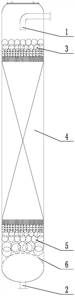
[0043] (1) Hexafluoroethane purification: after the hexafluoroethane raw material is vaporized by the vaporizer, the hexafluoroethane raw material gas is obtained; after the hexafluoroethane raw material gas is decompressed to 0.35±0.15MPa through the pressure reducing valve, the flow rate is controlled The temperature is 125±3kg / h, the temperature is 30±2.5℃, pass into the dryer for drying to obtain dry gas; pass the dry gas into the adsorber for adsorption and impurity removal, and then pass into the compressor to compress to 2.35±0.15 MPa, then pass into the condenser for liquefaction, pass the obtained crude hexafluoroethane into the intermediate product storage tank for storage; finally pass the crude hexafluoroethane in the intermediate product storage tank into the rectification device for rectification Purification to obtain high-purity hexafluoroethane; ...

Embodiment 2

[0051] A method for semiconductor etching utilizing high-purity hexafluoroethane, comprising the following steps:

[0052] (1) Hexafluoroethane purification: after the hexafluoroethane raw material is vaporized by the vaporizer, the hexafluoroethane raw material gas is obtained; after the hexafluoroethane raw material gas is decompressed to 0.35±0.15MPa through the pressure reducing valve, the flow rate is controlled The temperature is 125±3kg / h, the temperature is 30±2.5℃, pass into the dryer for drying to obtain dry gas; pass the dry gas into the adsorber for adsorption and impurity removal, and then pass into the compressor to compress to 2.35±0.15 MPa, then pass into the condenser for liquefaction, pass the obtained crude hexafluoroethane into the intermediate product storage tank for storage; finally pass the crude hexafluoroethane in the intermediate product storage tank into the rectification device for rectification Purification to obtain high-purity hexafluoroethane; ...

Embodiment 3

[0059] A method for semiconductor etching utilizing high-purity hexafluoroethane, comprising the following steps:

[0060] (1) Hexafluoroethane purification: after the hexafluoroethane raw material is vaporized by the vaporizer, the hexafluoroethane raw material gas is obtained; after the hexafluoroethane raw material gas is decompressed to 0.35±0.15MPa through the pressure reducing valve, the flow rate is controlled The temperature is 125±3kg / h, the temperature is 30±2.5℃, pass into the dryer for drying to obtain dry gas; pass the dry gas into the adsorber for adsorption and impurity removal, and then pass into the compressor to compress to 2.35±0.15 MPa, then pass into the condenser for liquefaction, pass the obtained crude hexafluoroethane into the intermediate product storage tank for storage; finally pass the crude hexafluoroethane in the intermediate product storage tank into the rectification device for rectification Purification to obtain high-purity hexafluoroethane; ...


PUM

PropertyMeasurementUnit
diameteraaaaaaaaaa
diameteraaaaaaaaaa
thicknessaaaaaaaaaa

Abstract

The invention relates to the field of semiconductor devices, and discloses a method for performing semiconductor etching by using high-purity hexafluoroethane, which comprises the following steps of: drying hexafluoroethane raw material gas, introducing the dried gas into an adsorber with a special structure for adsorption and impurity removal, and sequentially performing liquefaction and rectification purification to obtain the high-purity hexafluoroethane, and after plasma is formed by etching gas containing high-purity hexafluoroethane, dry etching is carried out on the semiconductor substrate covered with the patterned mask. According to the invention, the adsorber with a special structure is adopted to perform adsorption and impurity removal on the hexafluoroethane dry gas, and the distribution uniformity of the dry gas in the adsorber can be improved, so that the adsorption and impurity removal effect is improved, the hexafluoroethane with higher purity can be obtained, and the influence of impurities in the hexafluoroethane on the performance of a semiconductor device is reduced; meanwhile, the adsorber can improve the distribution uniformity of regeneration gas, so that the regeneration period of the molecular sieve is shortened, and the regeneration quality is improved.

Description

technical field [0001] The invention relates to the field of semiconductor devices, in particular to a method for semiconductor etching using high-purity hexafluoroethane. Background technique [0002] Semiconductor etching technology uses physical, chemical or a combination of the two methods to purposely remove the film layer that is not covered by the resist (mask), thereby forming the same pattern on the film as the mask. One of the important steps in the manufacture of semiconductor devices. At present, semiconductor etching methods mainly include wet etching and dry etching. Wet etching uses the chemical reaction between chemical reagents and the material to be etched for etching, which has the problems of poor anisotropy of chemical reaction, easy damage to the mask by chemical reagents, and difficulty in accurately controlling the pattern. Dry etching is to expose the surface of the silicon wafer to a specific gaseous state to generate plasma, use the plasma to pas...

Claims


Application Information

Patent Timeline
Patent Type & Authority Applications(China)
IPC IPC(8): H01L21/311H01L21/3065B01D53/26B01D53/04
CPCH01L21/31116H01L21/31144H01L21/3065B01D53/04B01D53/26B01D53/0407
Inventor 甘华平王战思秦远望李涛孟恒
Owner 宿州伊维特新材料有限公司
Why Eureka
Try Eureka