Semiconductor structure and forming method thereof

A technology of semiconductor and gate structure, applied in the field of semiconductor structure and its formation, can solve the problem that the breakdown voltage and on-current are difficult to increase at the same time, and achieve the effects of improving electrical performance, reducing on-resistance, and large on-current

Pending Publication Date: 2022-07-29
SEMICON MFG INT (SHANGHAI) CORP +1
View PDF0 Cites 0 Cited by
  • Summary
  • Abstract
  • Description
  • Claims
  • Application Information

AI Technical Summary

Problems solved by technology

[0004] However, it is difficult to increase the breakdown voltage (Breakdown Voltage) and conduction current of LDMOS devices at the same time

Method used


Image

  • Semiconductor structure and forming method thereof
  • Semiconductor structure and forming method thereof
  • Semiconductor structure and forming method thereof

Examples


Embodiment Construction

[0013] It can be known from the background art that the semiconductor structure formed at present still has the problem of poor electrical performance. Now combined with a method for forming a semiconductor structure, the reasons for the poor electrical performance of the semiconductor structure are analyzed.

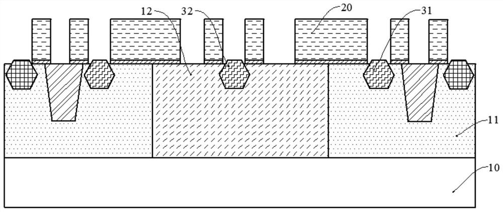
[0014] refer to figure 1 , showing a schematic structural diagram of a semiconductor structure.

[0015] The semiconductor structure shows a design of an LDMOS, and the semiconductor structure includes: a substrate in which adjacent well regions 11 and drift regions 12 are formed; a gate structure 20 located in the well region 11 On the substrate at the junction with the drift region 12; the source region 31 is located in the well region 11 on one side of the gate structure 20; the drain region 32 is located in the drift region 12 on the other side of the gate structure 20 .

[0016] The breakdown voltage (Break down Voltage) of LDMOS devices is one of the research f...


PUM


Abstract

The invention discloses a semiconductor structure and a forming method thereof, and the semiconductor structure comprises a gate structure which is located on a substrate and is parallel to the surface of the substrate and is perpendicular to the extending direction of the gate structure as the transverse direction; the drain electrode is positioned on one side of the gate structure; the first drift region and the drain electrode are located on the same side of the gate structure, and the projection of the first drift region in the substrate covers the projection of the drain electrode in the substrate; the second drift region is located at the end, close to the drain electrode, of the gate structure, the first drift region and the second drift region are spaced in the transverse direction, and the ion doping concentration of the second drift region is higher than that of the first drift region. In the embodiment of the invention, the projection of the first drift region in the substrate covers the projection of the drain electrode in the substrate, so that the drain electrode voltage drop borne by the first drift region is relatively high, and the breakdown voltage of the LDMOS is relatively high; and the ion doping concentration of the second drift region is higher than that of the first drift region, so that the on-resistance of the first drift region is relatively small, and the on-current of the LDMOS is relatively large.

Description

technical field [0001] Embodiments of the present invention relate to the field of semiconductor manufacturing, and in particular, to a semiconductor structure and a method for forming the same. Background technique [0002] With the rapid development of semiconductor manufacturing technology, semiconductor devices are developing in the direction of higher component density, higher integration and higher performance. A power semiconductor device (Power Electronic Device) is a high-power electronic device mainly used in power conversion and control circuits of power equipment (usually refers to a current of tens to thousands of amperes and a voltage of hundreds of volts or more). [0003] Among them, LDMOS (Laterally Diffused Metal Oxide Semiconductor, Laterally Diffused Metal Oxide Semiconductor) is a power device with a double diffusion structure, which is often used in radio frequency power circuits. control requirements, etc. Lateral Double Diffusion Field Effect Transi...

Claims


Application Information

Patent Timeline
Patent Type & Authority Applications(China)
IPC IPC(8): H01L29/06H01L29/78H01L21/336
CPCH01L29/0619H01L29/0684H01L29/7823H01L29/66681
Inventor 王孝远张进书宋辉潘梓诚
Owner SEMICON MFG INT (SHANGHAI) CORP
Why Eureka
Try Eureka