Self-powered MSM type ZnO-based ultraviolet photoelectric detector and preparation method thereof

A technology of electrical detectors and ultraviolet light, which is applied in the direction of circuits, electrical components, semiconductor devices, etc., can solve the problems of unsatisfactory band-pass response and low responsivity of MSM type ultraviolet detectors, and achieve the effect of improving device responsivity

Pending Publication Date: 2022-08-09
SOUTH CHINA UNIV OF TECH
View PDF0 Cites 0 Cited by
  • Summary
  • Abstract
  • Description
  • Claims
  • Application Information

AI Technical Summary

Problems solved by technology

[0005] The invention provides a self-powered MSM-type ZnO-based ultraviolet photodetector with a band-pass filtering function and a preparation method thereof, which are used to solve the problems of low responsivity of the MSM-type ultraviolet detector, the need for an external power supply, and the inability to meet the band-pass response, etc.

Method used


Image

  • Self-powered MSM type ZnO-based ultraviolet photoelectric detector and preparation method thereof
  • Self-powered MSM type ZnO-based ultraviolet photoelectric detector and preparation method thereof
  • Self-powered MSM type ZnO-based ultraviolet photoelectric detector and preparation method thereof

Examples


Embodiment 1

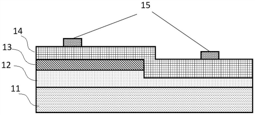
[0031] like figure 1 As shown, this embodiment is a self-powered MSM-type ZnO-based ultraviolet photodetector with band-pass filtering function. The device structure is grown by metal organic chemical vapor deposition and radio frequency magnetron sputtering, including a sapphire substrate 11, An n-type GaN buffer layer 12 , a p-type GaN active layer 13 , an n-type ZnO active layer 14 , and a Pt electrode (ie, a Schottky contact electrode) 15 .

[0032] In the above device structure, the n-type GaN buffer layer 12 is deposited on the substrate 11; the p-type GaN active layer 13 only covers part of the n-type GaN buffer layer 12, and the transition from the n-type GaN buffer layer to the p-type GaN has As a continuous top layer, the n-type ZnO active layer is partly covered on the p-type GaN active layer 13, and the other part is covered on the n-type GaN buffer layer 12, so that the two parts of the n-type ZnO have The source layer 14 is affected by the underlying GaN layer t...

Embodiment 2

[0057] The structure of this embodiment is basically the same as that of the ultraviolet light detection device of Embodiment 1, the difference is that the active layer 13 is made of p-type Al. 0.1 Ga 0.9 N, the Schottky contact electrode 15 uses an Au electrode.

[0058] The preparation method of the detector in this embodiment specifically includes the following steps:

[0059] S1. Cleaning the substrate: first, soak the substrate in a solution of HCl:deionized water = 1:1 for 10 minutes to remove surface oxides, then put in acetone and isopropanol for ultrasonic cleaning for 5 minutes, and rinse with deionized water The sample was blown dry 5 times with nitrogen until the surface was free of water beads.

[0060] S2. Growth of buffer layer and active layer: depositing n-type GaN with a thickness of 700 nm on the sapphire substrate 11 as a buffer layer 12 and p-type Al with a thickness of 80 nm on the sapphire substrate 11 by metal organic chemical vapor deposition 0.1 Ga...


PUM

PropertyMeasurementUnit
Thicknessaaaaaaaaaa
Thicknessaaaaaaaaaa

Abstract

The invention relates to the technical field of semiconductors, in particular to a self-powered MSM type ZnO-based ultraviolet photoelectric detector and a preparation method thereof, and the detector comprises a substrate, an n-type buffer layer, a p-type active layer, an n-type active layer and two electrodes; the n-type buffer layer is deposited on the substrate; the p-type active layer only covers part of the n-type buffer layer to form a step from the n-type buffer layer to the p-type active layer; the n-type active layer serves as a continuous top layer, one part of the n-type active layer covers the p-type active layer, and the other part of the n-type active layer covers the n-type buffer layer, so that the two parts of the n-type active layer generate unequal electron concentrations, and a space charge region for separating photon-generated carriers is generated at the step; the two electrodes are distributed on the two sides of the step respectively, and a space charge region formed by a Schottky contact barrier between the two electrodes further separates photo-induced electron-hole pairs. Compared with the prior art, the device has the advantages of simple structure, back incidence band-pass response, high light responsivity, high response speed and no need of external bias voltage.

Description

technical field [0001] The invention relates to the technical field of semiconductors, in particular to a self-powered MSM type ZnO-based ultraviolet photodetector with band-pass filtering function and a preparation method thereof. Background technique [0002] Ultraviolet detection technology has broad application prospects in various practical applications such as optoelectronic circuits, fire detection, atmospheric environment monitoring and optical communication. Currently, UV light detectors based on third-generation wide-bandgap semiconductors have attracted widespread attention due to their advantages such as no visible light interference, no need for filters, high stability, and strong radiation resistance. As a direct bandgap semiconductor, ZnO has a forbidden band width of 3.37 eV and a transmittance of more than 90% in the visible light band. GaN, which also has a direct energy gap, has a band gap slightly larger than that of ZnO (3.42 eV). Due to its excellent p...

Claims


Application Information

Patent Timeline
IPC IPC(8): H01L31/0352H01L31/0224H01L31/108H01L31/18
CPCH01L31/035281H01L31/035272H01L31/022408H01L31/1085H01L31/18Y02P70/50
Inventor 卢振亚林银华
Owner SOUTH CHINA UNIV OF TECH
Why Eureka
Try Eureka