Production method for flat panel display

A flat-panel display and manufacturing method technology, applied in semiconductor/solid-state device manufacturing, instruments, electric solid-state devices, etc., can solve problems such as difficulty in polysilicon thin films

Inactive Publication Date: 2005-01-19
SONY CORP
View PDF1 Cites 1 Cited by
  • Summary
  • Abstract
  • Description
  • Claims
  • Application Information

AI Technical Summary

Problems solved by technology

However, in these various manufacturing processes of semiconductor devices, it is difficult for an amorphous silicon thin film to become a polysilicon thin film having excellent film properties by polycrystallization due to the influence of hydrogen contained in the amorphous silicon thin film

Method used


Image

  • Production method for flat panel display
  • Production method for flat panel display
  • Production method for flat panel display

Examples


Embodiment Construction

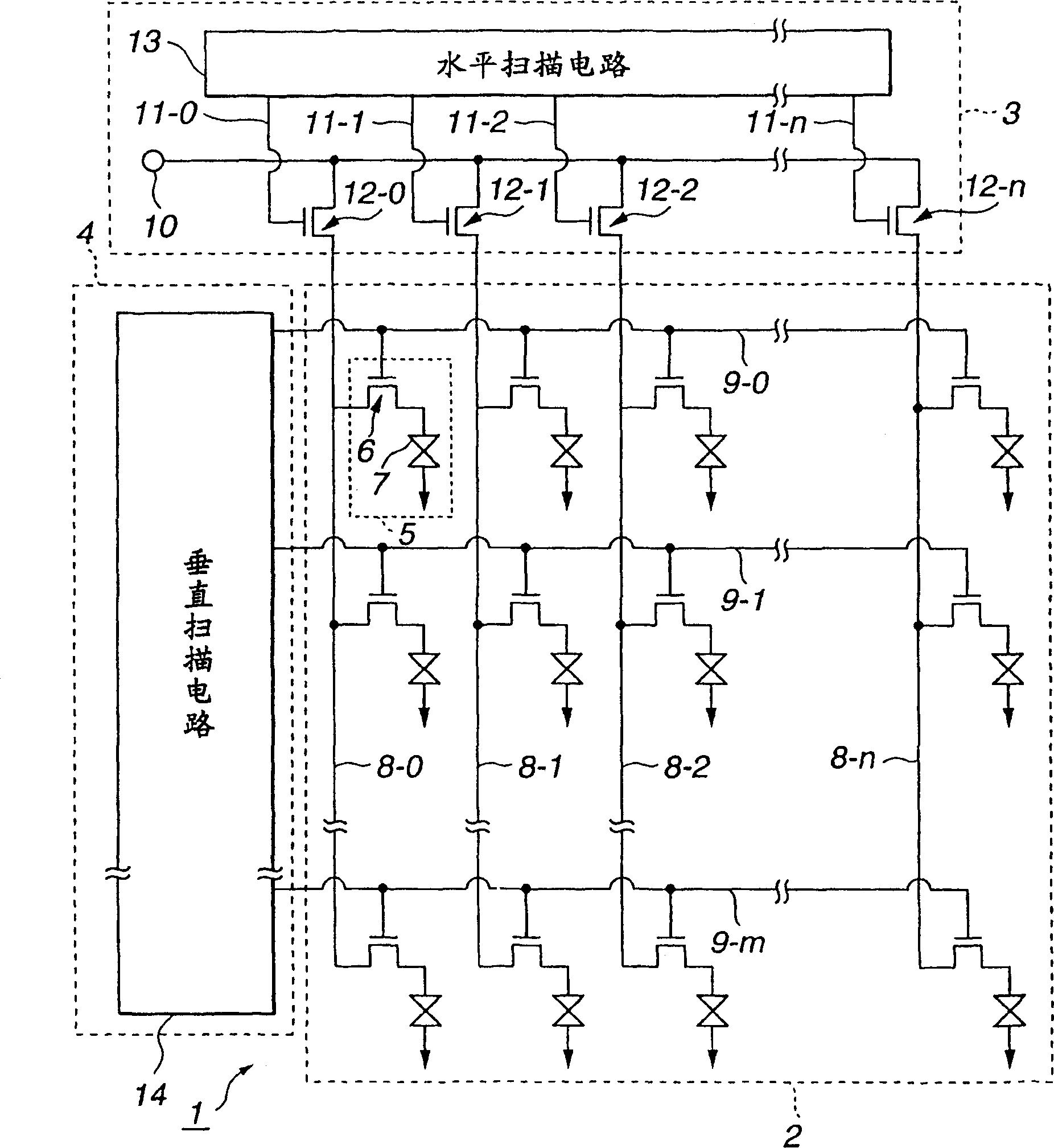
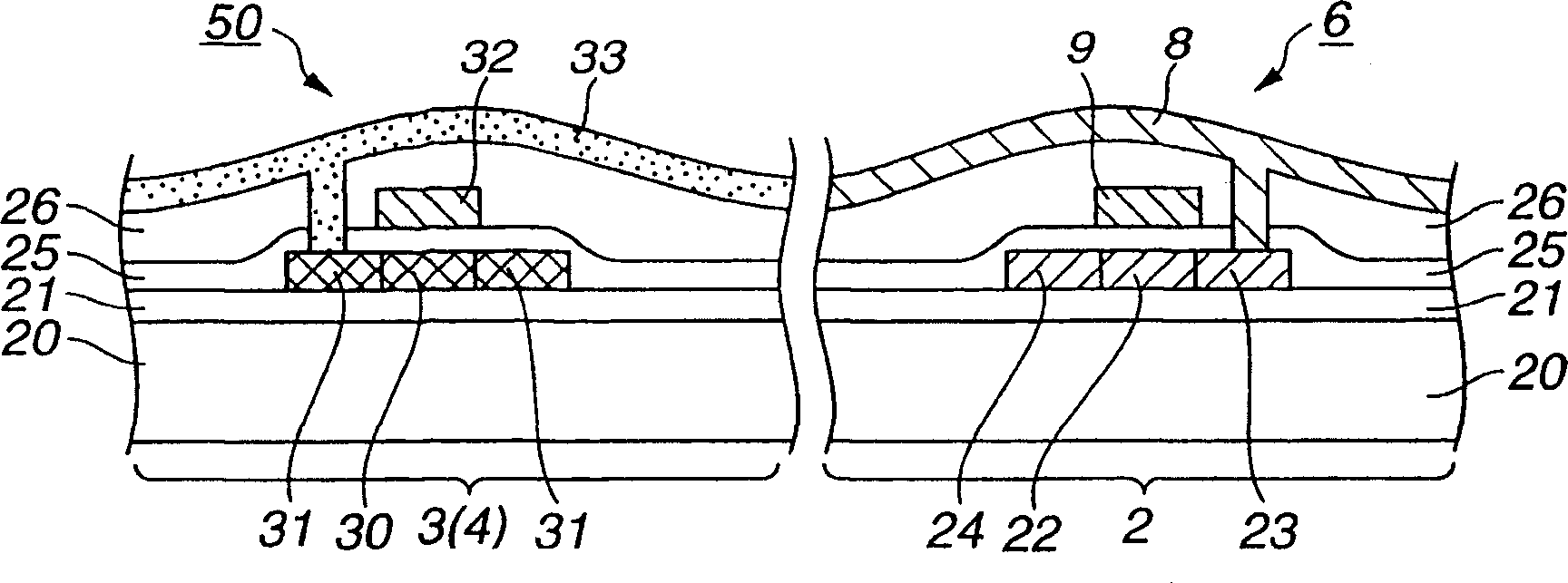
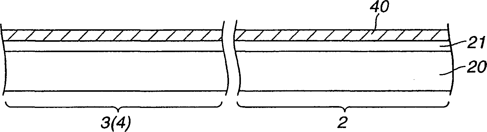
[0038] The invention will be described in detail below with the aid of the drawings. The present invention is suitably used in a liquid crystal display panel as a flat panel display.

[0039] Such as figure 1 As shown, the liquid crystal display panel 1 to which the present invention is applied includes a pixel area 2, a horizontal scanning area 3 and a vertical scanning area 4, which are formed on the same glass substrate.

[0040] The horizontal scanning area 3 includes a horizontal scanning circuit 13 and (n+1) transistors 12 - 0 to 12 -n, and the (n+1) horizontal selection signal lines 11 - 0 to 11 -n are driven by the horizontal scanning circuit 13 . These horizontal selection signal lines 11-0 to 11-n are connected to the gates of the corresponding transistors 12-0 to 12-n.

[0041] The video signal terminal 10 is connected to one of the sources / drains of all transistors 12-0~12-n, and the corresponding video signal lines 8-0~8-n are connected to the sources / drains of ...


PUM

PropertyMeasurementUnit
surface temperatureaaaaaaaaaa
thicknessaaaaaaaaaa
thicknessaaaaaaaaaa

Abstract

A production method for a flat panel display, capable of producing with a high reliability the TFT of a pixel unit and the TFT of a scanning unit, the method comprising a thin film forming step for forming an amorphous silicon thin film on a substrate consisting of a pixel unit and a drive unit, a dehydrogenation annealing step of applying a laser beam to an amorphous silicon thin film formed on the drive unit but not to an amorphous silicon thin film formed on the pixel unit out of the amorphous silicon thin film to release hydrogen contained in the amorphous silicon thin film on the drive unit, and then a crystallization annealing step of further applying a laser beam to the amorphous silicon thin film on the drive unit to change the amorphous silicon thin film on the drive unit to a polycrystalline silicon thin film.

Description

technical field [0001] The present invention relates to a method of manufacturing a flat panel display, and more particularly to a method of changing an amorphous silicon thin film formed on a substrate on which a pixel region and a driving region are established into a polysilicon thin film having excellent film properties. Background technique [0002] Liquid crystal display panels have been widely used as display devices for various electronic devices. As such a liquid crystal panel, a liquid crystal panel in the form of an active matrix in which switching of pixels is performed by turning on and off a switching element formed on each pixel in a display area has been used. [0003] In the above-mentioned active matrix type liquid crystal display, a thin film transistor (TFT) using an amorphous silicon thin film in a channel portion has been used as a switching element in a pixel region. This is because the amorphous silicon thin film can be uniformly formed over a large ...

Claims


Application Information

Patent Timeline
Patent Type & Authority Patents(China)
IPC IPC(8): G02F1/1362G02F1/1368H01L21/20H01L21/77H01L21/84H01L27/12
CPCG02F1/1368H01L27/1285H01L27/1214G02F2202/104H01L21/2026G02F1/13454H01L27/12H01L21/02686H01L21/02488H01L21/02422H01L21/02678H01L21/02532H01L21/02691G02F1/1333
Inventor 野口隆碓井節夫中嵨英晴
Owner SONY CORP
Why Eureka
Try Eureka