Two-dimensional photon crystal polarization beam dividing device
A two-dimensional photonic crystal, polarization beam splitter technology, applied in polarization components, optics, instruments, etc., can solve problems such as unfavorable integrated optics and volume limitations
- Summary
- Abstract
- Description
- Claims
- Application Information
AI Technical Summary
Problems solved by technology
Method used
Image
Examples
Embodiment Construction
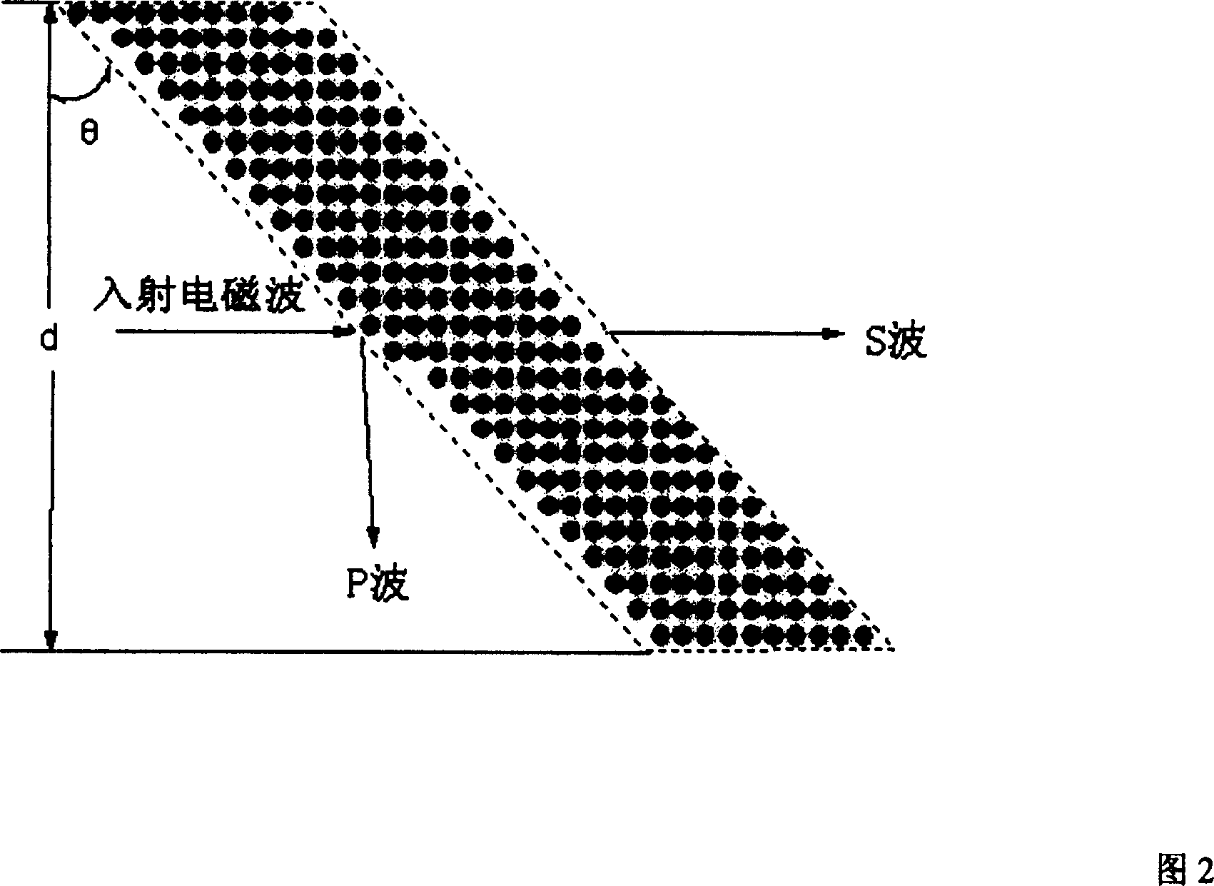
[0019] As shown in Figure 2, the incident electromagnetic wave source is a single slit diffracted wave source with a slit width of 240a and a wavelength of 10a in the background medium (the lattice constant a is used as the unit of length in the following work).
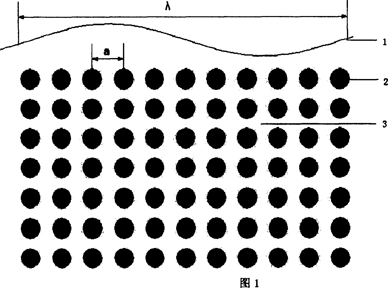
[0020] On the two-dimensional plane, silicon (refractive index n=3.4) is selected as the background medium, and the dielectric rod array is air (refractive index n=1.0). The overall profile of the beam splitter is a parallelogram (shown by a dotted line in Figure 2), wherein the length of the two short sides parallel to the incident direction of electromagnetic waves is 10a, the distance d=246a, and the angle between the long side and the vertical line of the short side θ=47° , rod radius 0.39a. The incident wave (the size of the S wave and the P wave in the incident wave is equal) passes through the structure and emerges as two polarized waves, the S wave and the P wave. The directions are 0 degrees and 86 degrees c...
PUM
 Abstract
Description
Claims
Application Information


