Patterned sapphire substrate with nonpolar and semipolar surface, visual light communication light source with nonpolar and semipolar surface and preparation method thereof

A sapphire substrate and visible light communication technology, applied in the field of visible light communication, can solve the problems of restricted modulation bandwidth, high background carrier concentration, insufficient light absorption, and slow response speed, so as to increase the proportion and rate of radiative recombination and improve the visible light Communication performance, the effect of reducing the formation of polycrystals

Active Publication Date: 2019-10-15
NANJING UNIV
View PDF4 Cites 5 Cited by
  • Summary
  • Abstract
  • Description
  • Claims
  • Application Information

AI Technical Summary

Problems solved by technology

The modulation bandwidth of the LED is mainly determined by the RC time constant and the recombination lifetime of the carrier radiation. By reducing the size of the LED, the junction capacitance and the RC time constant can be effectively reduced, thereby improving the modulation bandwidth of the LED. However, this method also It will reduce the light output power of the LED; another way to increase the modulation bandwidth of the LED is to reduce the carrier radiation recombination lifetime. Studies have shown that the relationship between the modulation bandwidth of the LED and the current density is close to a linear relationship. With the increase of the current density, the load The recombination lifetime of the carriers gradually decreases, but when the curren

Method used


Image

  • Patterned sapphire substrate with nonpolar and semipolar surface, visual light communication light source with nonpolar and semipolar surface and preparation method thereof
  • Patterned sapphire substrate with nonpolar and semipolar surface, visual light communication light source with nonpolar and semipolar surface and preparation method thereof
  • Patterned sapphire substrate with nonpolar and semipolar surface, visual light communication light source with nonpolar and semipolar surface and preparation method thereof

Examples


Embodiment 1

[0054] The preparation method of the visible light communication light source with non-polar and semi-polar surfaces comprises the steps of:

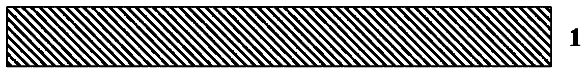
[0055] (1) A 2-inch r-plane sapphire substrate 1 is selected. The basic performance parameters of the r-plane sapphire substrate are as follows: the average half-peak width is 19.4arcsec; the dislocation density is 5.6×10 3 cm -3 ; The average transmittance when the wavelength is greater than 300nm is greater than 80%; Optical uniformity Δn = 6.6 × 10 -5 ; The average surface roughness is 0.49nm.

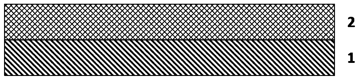
[0056] (2) Using PECVD technology to grow a SiO on a sapphire substrate 2 The dielectric layer 2 has a thickness of 200nm.

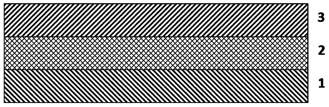
[0057] (3) Spin-coat the photoresist 3 on the above-mentioned substrate. The photoresist is reversed glue AZ5214, the spin-coating speed is 600rpm / 8000rpm, the time is 10s / 40s, and the pre-baking is performed on a hot plate at 90°C for 1 minute. Due to the use of reverse glue, a two-step exposure method is used. Fir...

Embodiment 2

[0070] The preparation method of the visible light communication light source with non-polar and semi-polar surfaces comprises the steps of:

[0071] (1) A 2-inch r-plane sapphire substrate 1 is selected. The basic performance parameters of the r-plane sapphire substrate are as follows: the average half-peak width is 19.4arcsec; the dislocation density is 5.6×10 3 cm -3 ; The average transmittance when the wavelength is greater than 300nm is greater than 80%; Optical uniformity Δn = 6.6 × 10 -5 ; The average surface roughness is 0.49nm.

[0072] (2) Using PECVD technology to grow a SiO on a sapphire substrate 2 The dielectric layer 2 has a thickness of 200nm.

[0073] (3) Spin-coat the photoresist 3 on the above-mentioned substrate. The photoresist is reversed glue AZ5214, the spin-coating speed is 600rpm / 8000rpm, the time is 10s / 40s, and the pre-baking is performed on a hot plate at 90°C for 1 minute. Due to the use of reverse glue, a two-step exposure method is used. Fir...

Embodiment 3

[0085] The preparation method of the visible light communication light source with non-polar and semi-polar surfaces comprises the steps of:

[0086] (1) A 2-inch r-plane sapphire substrate 1 is selected. The basic performance parameters of the r-plane sapphire substrate are as follows: the average half-peak width is 19.4arcsec; the dislocation density is 5.6×10 3 cm -3 ; The average transmittance when the wavelength is greater than 300nm is greater than 80%; Optical uniformity Δn = 6.6 × 10 -5 ; The average surface roughness is 0.49nm.

[0087] (2) Using PECVD technology to grow a SiO on a sapphire substrate 2 The dielectric layer 2 has a thickness of 200nm.

[0088] (3) Spin-coat the photoresist 3 on the above-mentioned substrate. The photoresist is reversed glue AZ5214, the spin-coating speed is 600rpm / 8000rpm, the time is 10s / 40s, and the pre-baking is performed on a hot plate at 90°C for 1 minute. Due to the use of reverse glue, a two-step exposure method is used. Fir...


PUM

PropertyMeasurementUnit
Thicknessaaaaaaaaaa
Bottom widthaaaaaaaaaa
Cycleaaaaaaaaaa

Abstract

The invention discloses a visible light communication light source based on a nonpolar and semipolar surface and a corresponding patterned sapphire substrate. A sapphire substrate is selected to be processed into grating-shaped strip-shaped patterns; the angle of the side wall of a step is optimized in the etching process, and the angle of a growth surface of the next step is optimized; a barrierlayer is designed on the patterned sapphire substrate, and a silicon oxide film is adopted as an epitaxial barrier layer; a GaN layer, an N-type GaN layer, an InGaN/GaN multi-quantum well layer, an electronic barrier layer and a p-type GaN layer are sequentially grown by adopting a chemical vapor phase epitaxy method, and the growth method of the GaN layer, the N-type GaN layer, the InGaN/GaN multi-quantum well layer, the electronic barrier layer and the p-type GaN layer is disclosed. The influence of quantum-limited Stokes effect is weakened by utilizing the advantages of non-polar/semipolarsurface on III-group nitride polarization regulation, the overlapping of electron-hole wave functions on real space is increased, and the radiation recombination proportion and the rate of current carriers are improved, and therefore, the method provided by the invention is suitable for effectively improvement of the visible light communication performances by adopting the nonpolar and semipolar surface technologies.

Description

technical field [0001] The invention relates to a patterned sapphire substrate with non-polar and semi-polar surfaces, a light source for visible light communication and a preparation method thereof, belonging to the field of visible light communication. Background technique [0002] At present, the modulation bandwidth of GaN-based LEDs epitaxy on c-plane sapphire is only a dozen megahertz (MHz) to tens of megahertz, which fundamentally restricts the communication rate of VLC integrated chips. The modulation bandwidth of the LED is mainly determined by the RC time constant and the recombination lifetime of the carrier radiation. By reducing the size of the LED, the junction capacitance and the RC time constant can be effectively reduced, thereby improving the modulation bandwidth of the LED. However, this method also It will reduce the light output power of the LED; another way to increase the modulation bandwidth of the LED is to reduce the carrier radiation recombination ...

Claims


Application Information

Patent Timeline
IPC IPC(8): H01L33/00H01L33/06H01L33/20H01L33/32H01L33/44
CPCH01L33/0075H01L33/06H01L33/20H01L33/32H01L33/44H01L2933/0058
Inventor 陶涛智婷刘斌谢自力陈鹏陈敦军修向前赵红张荣
Owner NANJING UNIV
Why Eureka
Try Eureka