
Structure self-aligning method for making infrared absorption layer of infrared snesor for micromechanical heat stack

A technology of infrared detector and infrared absorbing layer, which is applied in the field of micromechanics, can solve the problems of inaccurate positioning and high production cost, and achieve the effects of reducing production cost, improving performance and cost, and positioning accurately

Inactive Publication Date: 2002-04-03
SHANGHAI INST OF MICROSYSTEM & INFORMATION TECH CHINESE ACAD OF SCI
View PDF0 Cites 9 Cited by
  • Summary
  • Abstract
  • Description
  • Claims
  • Application Information

AI Technical Summary

Problems solved by technology

It is generally believed that a method similar to screen printing can be used, which requires the corresponding mask to be made separately. The production cost of this method is relatively high, and there is also the problem of inaccurate positioning during the production process.

Method used


Image

  • Structure self-aligning method for making infrared absorption layer of infrared snesor for micromechanical heat stack
  • Structure self-aligning method for making infrared absorption layer of infrared snesor for micromechanical heat stack
  • Structure self-aligning method for making infrared absorption layer of infrared snesor for micromechanical heat stack

Examples


Embodiment 1

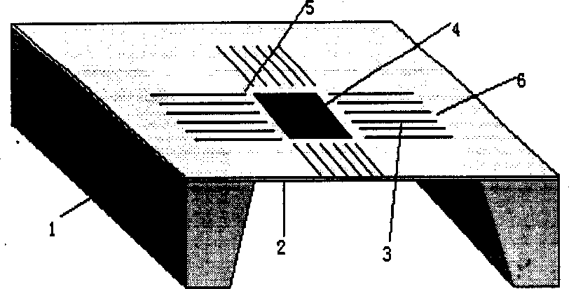
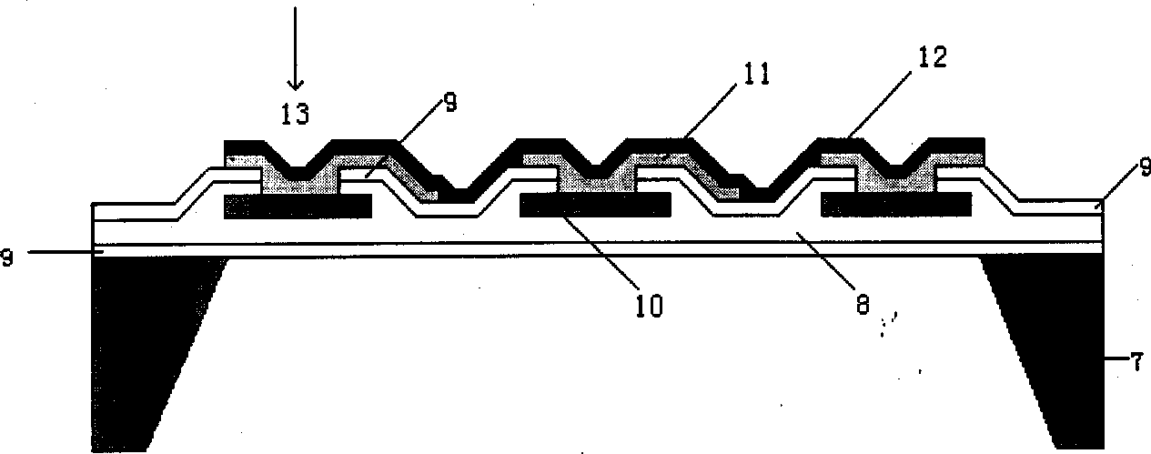
[0023] On the (100) monocrystalline silicon wafer 7, a layer of silicon nitride layer 9 is deposited by low-pressure chemical vapor phase (LPCVD), wherein the LPCVD deposition temperature is 800 ° C, and the thickness of the silicon nitride layer is 0.15 microns; LPCVD deposits polysilicon with a deposition temperature of 640°C and a thickness of 0.6 microns. All of it is thermally oxidized to form silicon oxide 8, and then a layer of silicon nitride is deposited by LPCVD with a thickness of 0.1 microns to form a "silicon nitride-silicon oxide-silicon nitride " sandwich layer.

[0024] Then use LPCVD to deposit a layer of polysilicon with a thickness of 0.6 microns, and carry out boron doping to make it have a certain surface resistance; then thermally oxidize its surface, photolithography the shape of a thermocouple silicon strip, use silicon oxide as a mask, and use The thermocouple silicon strip 10 is formed by dry etching, the strip width is ten to tens of microns, and the...

Embodiment 2

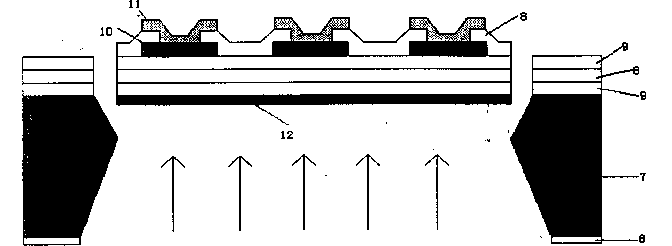
[0029] Thermally oxidize on a (100) single crystal silicon wafer to obtain a layer of silicon oxide with a thickness of 0.5 microns, and then deposit a layer of silicon nitride by LPCVD at a deposition temperature of 800°C with a thickness of 0.15 microns to obtain a layer of "oxidized Silicon-silicon nitride"composite dielectric film. Then use LPCVD to deposit a layer of polysilicon with a thickness of 0.6 microns. After boron doping, the polysilicon strip is photolithographically deposited, and metal aluminum is deposited on the surface to form a thermocouple pair with the polysilicon. When the structure is finally corroded, KOH is used for corrosion to obtain a thermal stack structure. All the other processes are the same as in Example 1.


PUM

PropertyMeasurementUnit
Thicknessaaaaaaaaaa
Thicknessaaaaaaaaaa
Thicknessaaaaaaaaaa

Abstract

A structure self-aligning method for preparing the infrared absorption layer of infrared sensor which is a micromechanical heat stack is disclosed. The front and back surfaces of monosilicon wafer are corroded at same time to obtain a window on the back of heat stack, whose sizes are similar to those of infrared absorption area. By the aligning action of said window, black body is evaporated and deposited on the back of heat stack in nitrogen atmosphere. Its advantages are simple process, low cost and precise location of infrared absorption layer.

Description

technical field [0001] The invention relates to a method for fabricating an infrared absorbing layer of a micromechanical thermopile infrared detector by a structural self-alignment method, which belongs to the field of micromechanics. Background technique [0002] Infrared detectors are the most basic and key components of infrared instruments. With the increasing application of infrared technology, higher requirements are placed on infrared detectors themselves. The thermopile infrared detector is a kind of thermal infrared detector, and its working principle is the Seebeck effect, which is the thermoelectric effect. When two different materials that make up a thermocouple form a closed loop, if there is a temperature difference between the two nodes, an electromotive force will be generated in the loop. Early thermopile infrared detectors were obtained by depositing thermocouple materials on plastic or alumina substrates by using mask vacuum coating method. The size of t...

Claims


Application Information

Patent Timeline
IPC IPC(8): G01J1/00G01J1/42H01L31/09
Inventor 徐峥谊熊斌王翊王跃林
Owner SHANGHAI INST OF MICROSYSTEM & INFORMATION TECH CHINESE ACAD OF SCI
Features
  • Generate Ideas
  • Intellectual Property
  • Life Sciences
  • Materials
  • Tech Scout
  • Unparalleled Data Quality
  • Higher Quality Content
  • 60% Fewer Hallucinations
Learn More