Method for providing dopant level for polysilicon for flash memory devices

A technology for writing memory and doping, which is applied in the field of flash memory devices and can solve the problems of charge gain and loss

Inactive Publication Date: 2002-09-11
CYPRESS SEMICON CORP
View PDF0 Cites 2 Cited by
  • Summary
  • Abstract
  • Description
  • Claims
  • Application Information

AI Technical Summary

Problems solved by technology

Therefore, it will lead to reliability problems and, when pr

Method used


Image

  • Method for providing dopant level for polysilicon for flash memory devices
  • Method for providing dopant level for polysilicon for flash memory devices
  • Method for providing dopant level for polysilicon for flash memory devices

Examples


Embodiment Construction

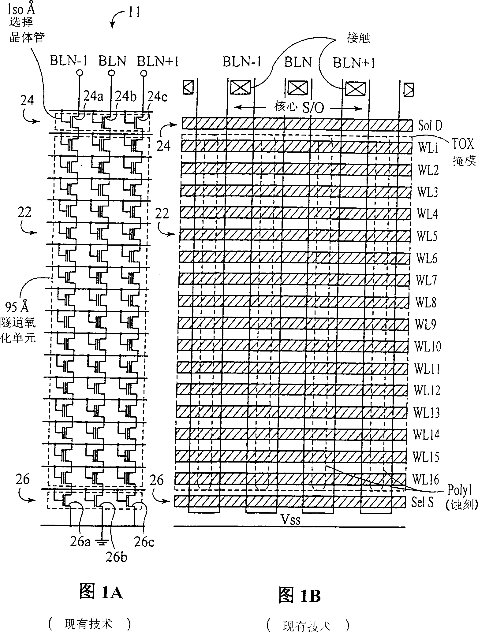
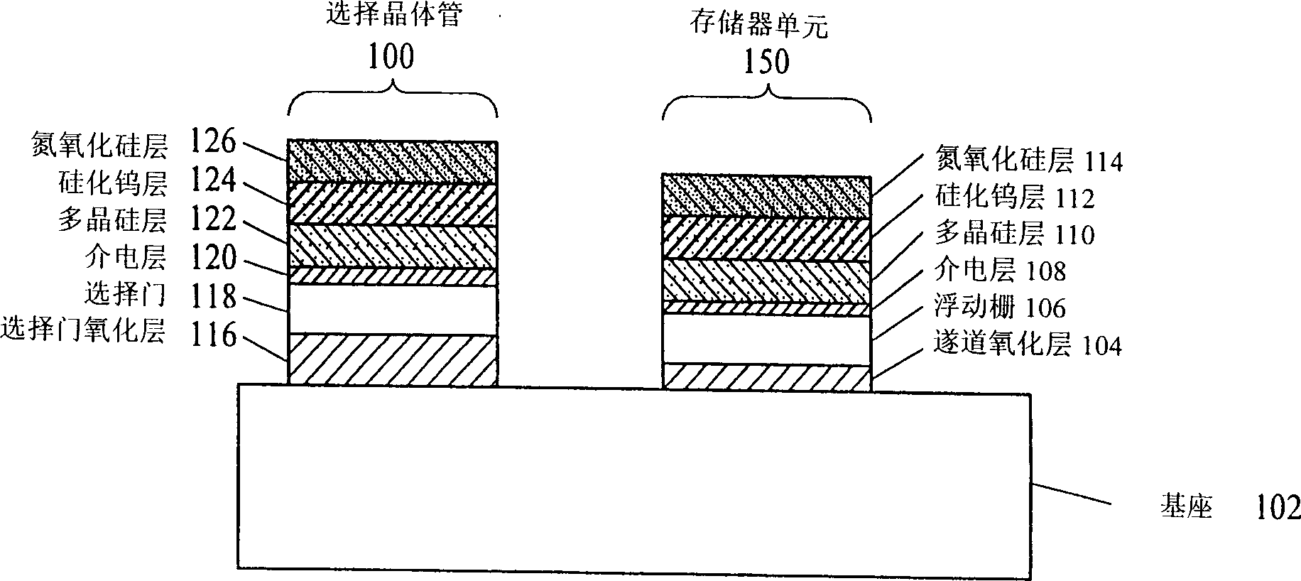
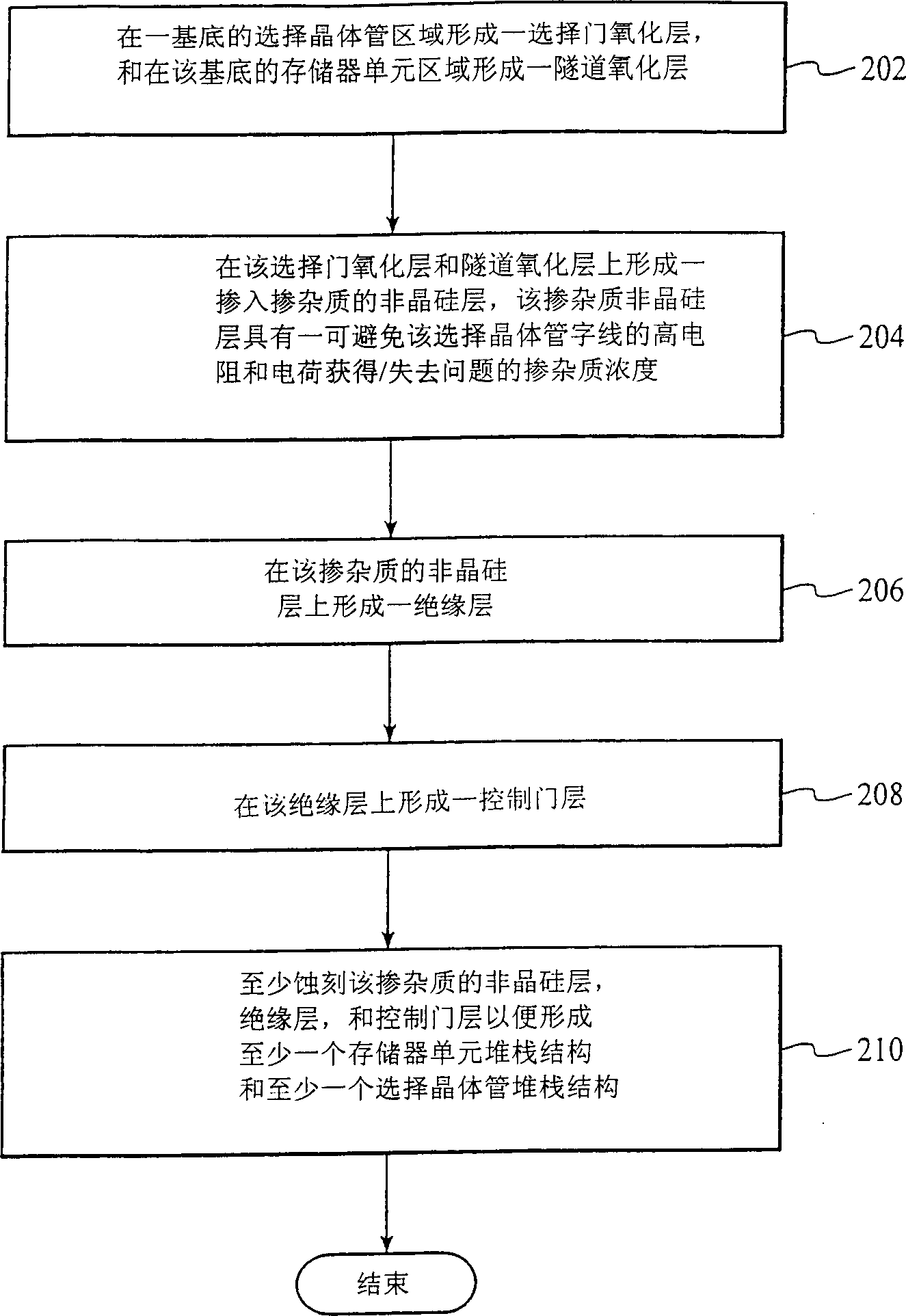
[0013] The present invention provides a method and NAND type flash memory device that provides a polysilicon dopant concentration that avoids high resistance and charge gain / loss problems of select transistor word lines. The description presented below will enable a person skilled in the art to make and use the invention and is provided in a patent application and its required text. Various modifications of this preferred embodiment will be clear to those skilled in the art and the general principles here will be applied to other embodiments. Therefore, the present invention is not limited to the scope disclosed by this embodiment, but is suitable for use with The broadest category in which the principles and characteristics described are consistent.

[0014] The method according to the invention will avoid the select transistor word line high resistance problem and charge gain / loss problem by providing the dopant concentration of the polysilicon layer, which is phosphorus dop...


PUM


Abstract

The invention provides a method and a NAND type flash memory device. The method includes: forming a selection gate oxide layer in a selection transistor region of a base, and forming a tunnel oxide layer in a memory cell area of ​​the base; forming a selection gate oxide layer on the selection gate oxide layer and the tunnel oxide layer. An amorphous silicon layer doped with impurities, the dopant concentration of the doped amorphous silicon layer can simultaneously avoid the problem of high resistance of the selection transistor word line, and can also avoid the problem of charge gain/charge loss; On the doped amorphous silicon layer, an insulating layer is formed; on the insulating layer, a control gate layer is formed; and at least the doped amorphous silicon layer, the insulating layer, and the control gate layer are etched. , to form at least one memory cell stack structure and at least one selection transistor stack structure. In a preferred embodiment, the polysilicon layer will form the floating gate of the flash memory cell and the select gate of the select transistor of the device, and the dopant concentration of the dopant phosphorus in the polysilicon layer is between 5× Between 1018 and 8×10¹⁹ ions/(cm)3(ions/cm3). With this dopant concentration, the contact resistance of the control gate of the select transistor becomes low, and therefore, the word line resistivity of the device can be made low. At the same time, since the dopant enters the tunnel oxide layer of the flash memory cell, the pollution of the tunnel oxide layer will be limited, and the contact surface between the floating gate and the tunnel oxide layer will be smooth, thus preventing charge gain/loss The problem. Therefore, the reliability of the device will be improved.

Description

technical field [0001] The present invention relates to a flash memory device, and more specifically, to a NAND type flash memory device. Background technique [0002] Semiconductor flash memory devices include NAND type flash memory devices. The memory device basically includes a high-density core region and a low-density edge region on a single base. As shown in FIG. 1A and FIG. 1B , the memory cells located in the core area are coupled together in the form of a NAND circuit. FIG. 1A is a schematic circuit diagram of the core area 11 ; and FIG. 1B is a plan view of the core area 11 . Core region 11 contains a memory cell region 22 bounded on one side by drain select transistor portion 24 and on the other side by source select transistor portion 26 . Each select transistor section 24 and 26 includes select gate transistors 24a-24c and 26a-26c, respectively, for selectively activating desired bit lines. [0003] FIG. 1C shows a cross-sectional view of a conventional stac...

Claims


Application Information

Patent Timeline
IPC IPC(8): H01L21/8247H01L27/115H01L29/788H01L29/792
CPCH10B41/35H10B41/30H10B99/00
Inventor K·K·H·张K·W·W·欧方浩
Owner CYPRESS SEMICON CORP
Why Eureka
Try Eureka