Reusable substance amount sensor in prodn. of organic luminous device

An organic light-emitting device and sensor technology, which can be applied to measurement devices, lighting devices, electrical devices, etc., can solve problems such as the limitation of crystal substance mass sensors, and achieve the effect of an effective manufacturing method.

Inactive Publication Date: 2002-12-04
GLOBAL OLED TECH
View PDF5 Cites 16 Cited by
  • Summary
  • Abstract
  • Description
  • Claims
  • Application Information

AI Technical Summary

Problems solved by technology

[0011] However, in a manufacturing environment where large numbers of organic light-emitting devices are repeatedly fabricated, replacement of "overloaded" crystalline mass sensors or crystalline mass sensors with cracked or peeled-off organic layers is severely limited. because the manufacturing system is configured to comprehensively provide the ability to produce all organic layers on many device structures, even fully enclosed OLEDs

Method used


Image

  • Reusable substance amount sensor in prodn. of organic luminous device
  • Reusable substance amount sensor in prodn. of organic luminous device
  • Reusable substance amount sensor in prodn. of organic luminous device

Examples


Embodiment Construction

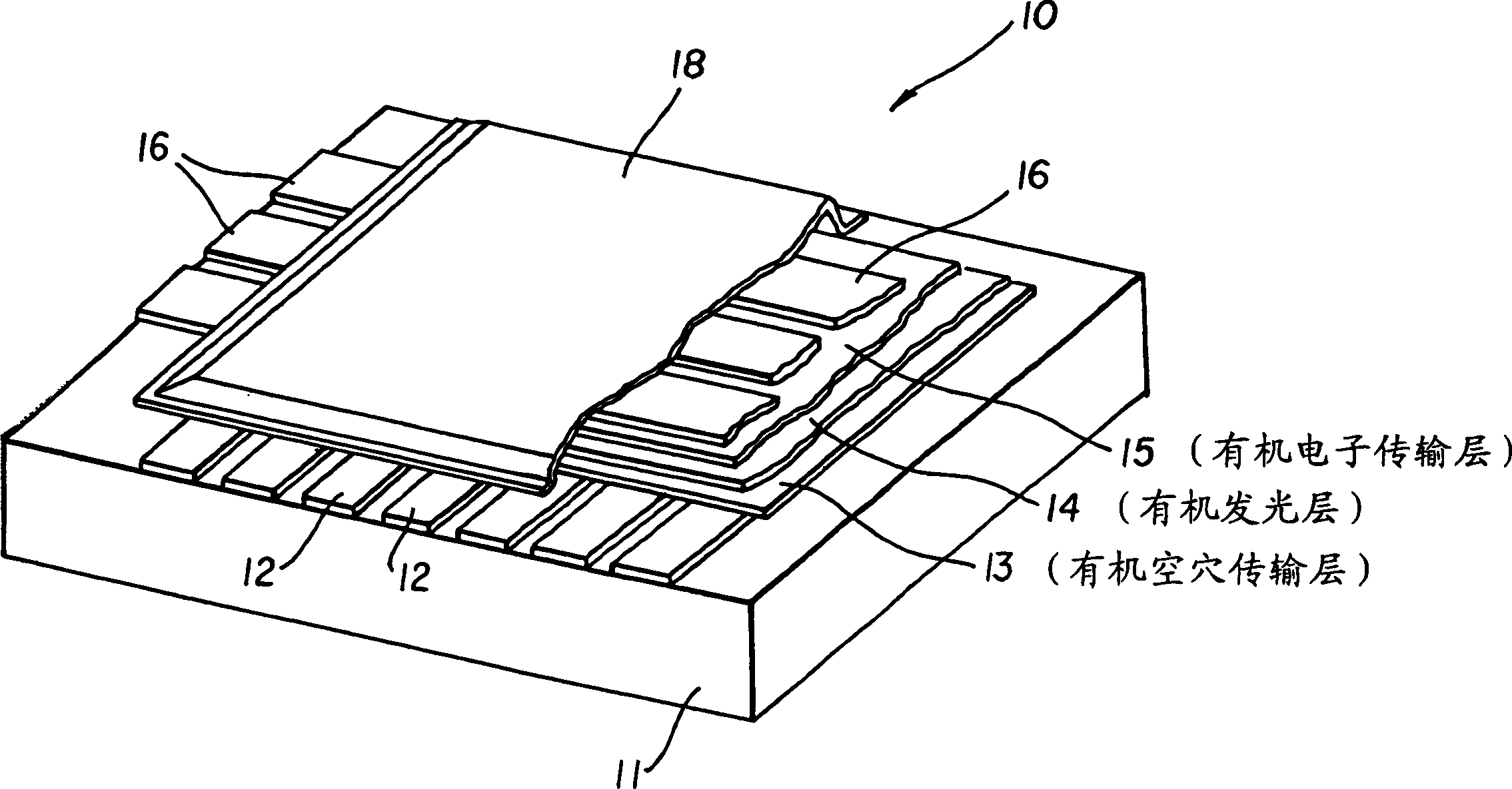
[0033] The term "substrate" herein refers to a light transmissive support on which are preformed a plurality of laterally spaced first electrodes (anodes), this substrate being the precursor to passive matrix OLEDs. The term "structure" here refers to the substrate after receiving a portion of the vapor-deposited organic layer, and indicates the difference between the active matrix arrangement and its passive matrix predecessor.

[0034] see figure 1 , figure 1 is a schematic perspective view showing a passive matrix organic light emitting device (OLED) 10 in which some elements have been peeled away to expose various layers.

[0035]A plurality of laterally spaced apart first electrodes 12 (also referred to as anodes) are formed on the light transmissive substrate 11 . An organic hole-transporting layer (HTL) 13 , an organic light-emitting layer (LEL) 14 and an organic electron-transporting layer (ETL) 15 are sequentially formed by physical vapor deposition, which will be d...


PUM


Abstract

The present invention relates to a method for controlling the deposition of organic materials in the manufacture of an organic light-emitting device, the method comprising: depositing an organic material in a deposition area to form a layer of an organic light-emitting device; setting a movable sensor, when the sensor moves to A signal indicative of the deposition rate and thickness of the organic material forming the layer is provided in the deposition zone and when covered during the deposition step. The method further includes: controlling the deposition of the organic material based on the signal to control the deposition rate and thickness of the organic material forming the layer; moving the movable sensor from the deposition area to a cleaning position; and removing the sensor from the movable sensor. Organic materials enable removable sensors that can be reused.

Description

Technical field: [0001] The present invention relates to methods of monitoring and controlling organic layers of organic materials formed by physical vapor deposition in the manufacture of organic light-emitting devices. Background technique: [0002] Organic light emitting devices, also known as organic electroluminescence light emitting devices, can be fabricated by sandwiching two or more organic layers between a first electrode and a second electrode. [0003] In a passive matrix (passive matrix) organic light-emitting device with a conventional structure, a plurality of laterally spaced light-transmitting anodes such as indium-tin-oxide (ITO) are formed on a light-transmitting substrate ( For example, on a glass substrate). Two or more organic layers are then sequentially formed using vapor deposition of respective organic materials from respective sources in a chamber maintained at reduced pressure (typically less than 10-3 Torr). A plurality of laterally spaced cath...

Claims


Application Information

Patent Timeline
Patent Type & Authority Applications(China)
IPC IPC(8): H05B33/10C23C14/12C23C14/54G01B7/06H01L51/00H01L51/40H01L51/50
CPCC23C14/12C23C14/546G01B7/066H10K71/164H10K50/11H05B33/10
Inventor M·A·马库斯A·L·赫里钦S·A·范斯利克
Owner GLOBAL OLED TECH
Why Eureka
Try Eureka