
Semiconductor device

A technology of semiconductors and gate transistors, applied in semiconductor devices, logic circuits using semiconductor devices, electric solid state devices, etc., can solve problems such as inability to obtain suitable actions, difficulty in high precision, weakening of learning and memory, etc.

Inactive Publication Date: 2003-01-08
PANASONIC CORP
View PDF0 Cites 10 Cited by
  • Summary
  • Abstract
  • Description
  • Claims
  • Application Information

AI Technical Summary

Problems solved by technology

[0029] Second, when the neuronal element has a learning function, it is sometimes desirable to additionally clear or weaken the function of learning and memory
As a result, it is difficult to set the load factor in multiple steps and with high precision
Since precision is required in the setting of the load factor in the operation processing of the neuron network, it is difficult to set a fine load factor using the method shown in Fig. 46, and as a result, learning is difficult to converge in the action of the neuron element. Problems such as not being able to obtain suitable actions

Method used


Image

  • Semiconductor device
  • Semiconductor device
  • Semiconductor device

Examples


Embodiment 1

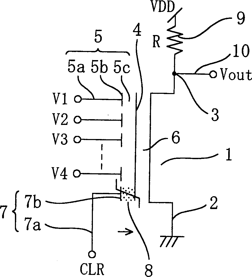
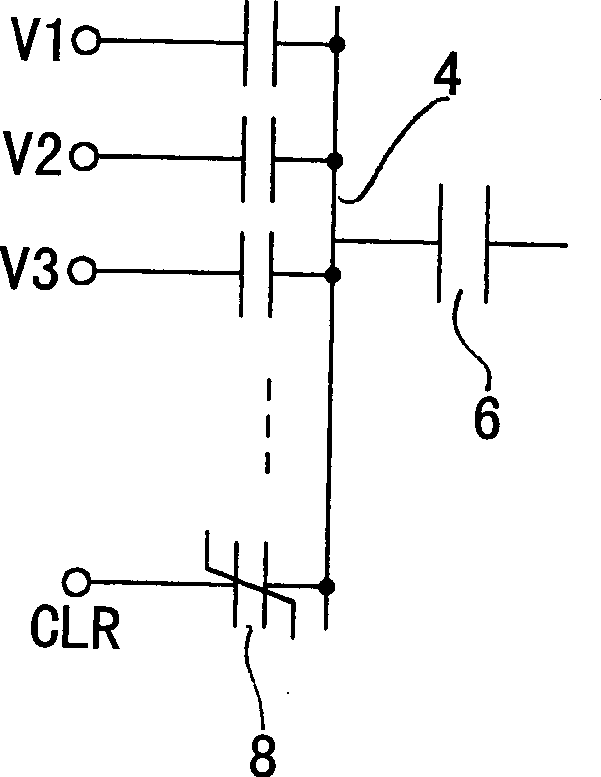
[0138] FIG. 1 is a schematic diagram showing a circuit configuration of a neuron element of a semiconductor device according to Embodiment 1 of the present invention. Fig. 3 is an equivalent circuit diagram in which only the capacitor portion of the neuron element of this embodiment is taken out.

[0139] The neuron element of this embodiment has an n-channel MIS transistor (NMISFET1) provided with a source terminal 2, a drain terminal 3, a gate insulating film 6, and a gate. Here, the gate of the NMISFET 1 is a floating gate 4 in a floating state that is not connected to other terminals. Both the source terminal 2 and the substrate area of ​​NMISFET 1 are connected to ground, and the drain terminal 3 is connected to the output terminal 10 . The output terminal 10 is connected to a power supply voltage supply unit for supplying a power supply voltage VDD via a load resistance element.

[0140] Also, n signal input sections 5 capacitively coupled to the floating gate 4 are pr...

Deformed example 2-

[0161] In the present embodiment, a circuit is constructed using a combination of NMISFET 1 and load resistance element 9 , but a p-type MIS transistor can be used instead of load resistance element 9 .

[0162] 6 is a schematic diagram showing a structure in which a neuron element, which is a semiconductor device in a second modified example of the first embodiment is provided. In the neuron element in this modified example, the load resistance element 9 in the structure shown in FIG. 1 is replaced by a p-channel type MIS transistor (PMISFET 11 ) connected in series with the NMISFET 1 . Further, the source terminal 12 of the PMISFET 11 is connected to a power supply voltage supply unit that supplies the power supply voltage VDD, and the drain terminal 13 of the PMISFET 11 is connected to the drain terminal 3 of the NMISFET 1 . The output terminal 10 is connected to the drain terminal 3 of the NMISFET 1 and the drain terminal 13 of the PMISFET 11 . In addition, the floating g...

Embodiment 2

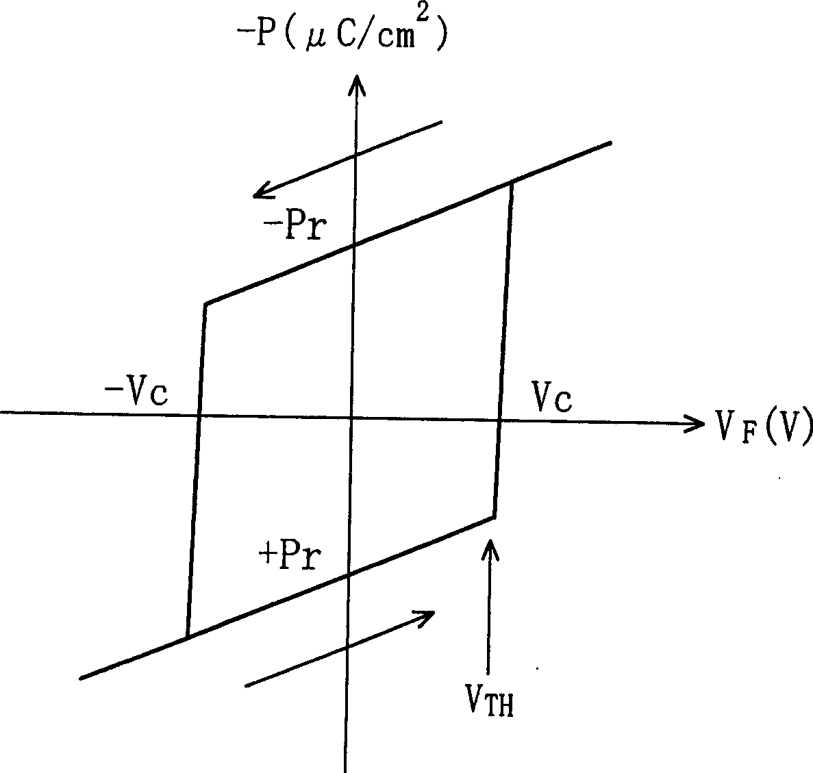
[0165] In the first embodiment, an element is designed in which the threshold voltage VTH of the NMISFET 1 is almost equal to the withstand voltage Vc of the ferroelectric film 8, but the element design can be performed in a manner different from that of the first embodiment. In this embodiment, the same circuit structure as that of Embodiment 1 is adopted with reference to FIGS. 1 and 7, but components designed in a different manner are used for explanation. That is, the circuit structure of the neuron element of this embodiment is shown in FIG. 1 .

[0166] FIG. 7 is a graph showing the voltage dependence (hysteresis loop) of the remnant polarization of the ferroelectric film 8 when a method different from that of Example 1 is adopted. For example, elements can be designed so that the threshold voltage VTH of the NMISFET 1 is smaller than the withstand voltage Vc of the ferroelectric film 8, and the potential VF of the floating gate 4 when the input voltages of the n signal ...


PUM


Abstract

In an electric potential generating device, a source of an N type MIS transistor is mutually connected to that of a P type MIS transistor and also connected to an output terminal. A drain of an N type MIS transistor 54 is connected to a power supply voltage supply portion for supplying power supply voltage VDD, and a drain of the P type MIS transistor is connected to a ground. In addition, a substrate potential of the N type MIS transistor is a ground voltage VSS, and that of a P type MIS transistor 56 is the power supply voltage VDD. Thus, it is constituted as a source follower circuit for taking output out of the source. It is possible, by utilizing this electric potential generating device, to obtain a logic transformation circuit for stably switching between NOR operation and NAND operation.

Description

technical field [0001] The present invention relates to a semiconductor device, and more particularly, to a semiconductor device functioning as a neuron element, a potential generator, a logic conversion circuit, etc., which are elements of an artificial neural network. Background technique [0002] The development of semiconductor integrated circuit technology in recent years has been astonishing, and various high-function logic integrated circuits have been developed in addition to memory elements alone. However, it can be said that these logic circuits have not progressed in the evolution of logic since the appearance of LSI, on the other hand, in terms of performing operations using binary signals. In today's semiconductor integrated circuits, in such binary calculations, very high-speed calculations can be performed for simple input calculations, but calculations that are easy for humans, such as pattern recognition and image processing, require a large amount of labor....

Claims


Application Information

Patent Timeline
Patent Type & Authority Applications(China)
IPC IPC(8): H01L27/10G11C27/00
CPCG11C11/54G11C27/005H01L2924/0002H01L2924/00H01L27/10
Inventor 上田路人丰田健治森田清之大塚隆
Owner PANASONIC CORP
Learn More