High frequency semiconductor device

A semiconductor, high-frequency technology, applied in the direction of semiconductor devices, semiconductor/solid-state device components, electric solid-state devices, etc., can solve the problems of high thermal resistance, high-power semiconductor chips can not be fully dissipated, and are in a high temperature state.

Inactive Publication Date: 2003-04-23
PANASONIC CORP
View PDF0 Cites 12 Cited by
  • Summary
  • Abstract
  • Description
  • Claims
  • Application Information

AI Technical Summary

Problems solved by technology

The problem is that due to the large thermal resistance of the ceramic multilayer substrate, the high-power semiconductor chip cannot be fully dissipated and is in a high temperature state.

Method used


Image

  • High frequency semiconductor device
  • High frequency semiconductor device
  • High frequency semiconductor device

Examples


no. 1 example

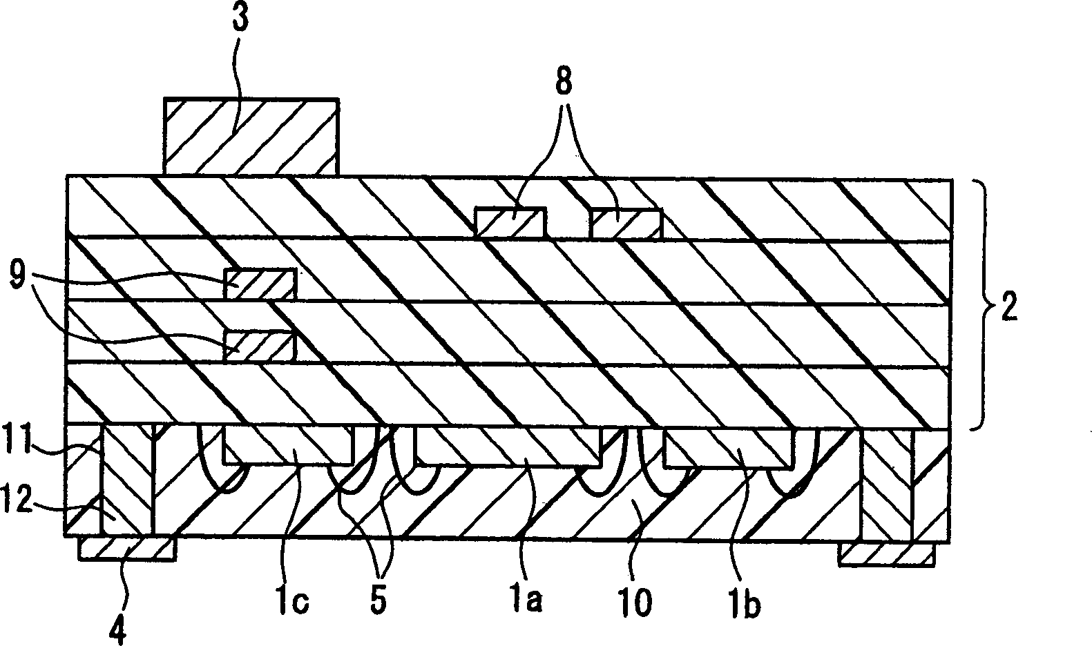
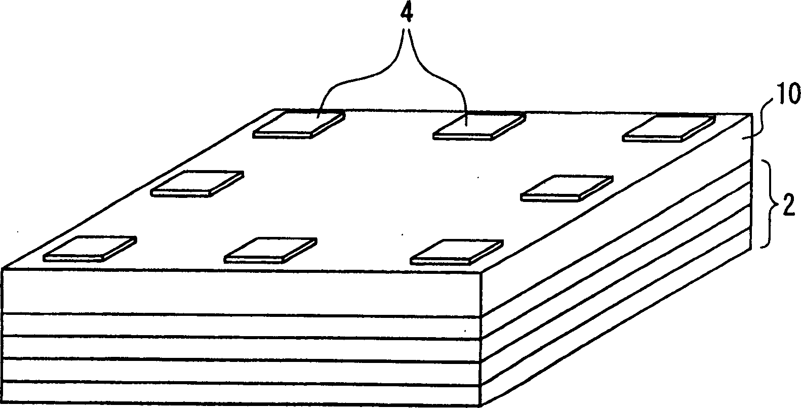
[0030] figure 1 is a cross-sectional view of the high-frequency semiconductor device in the first embodiment of the present invention; figure 2 is viewed from the back figure 1 Perspective view of a high-frequency semiconductor device.

[0031] figure 1 Middle: 1a is a gallium arsenide power semiconductor element as a power amplifier, 1b is a gallium arsenide semiconductor element as a switching element, and 1c is a silicon semiconductor element for circuit control. 2 is a non-shrinkable ceramic multilayer substrate, and its inner layer is provided with a printed resistor 8 and a printed capacitor 9 printed by a metal-containing paste material that are sintered at a low temperature. 3 is a chip component, which can be used for micro Components such as chip capacitors that adjust high-frequency circuit constants. 5 is a metal wire, and 10 is a composite resin material layer formed of an epoxy resin and an inorganic filler such as silicon. 4 is an external connection elect...

no. 2 example

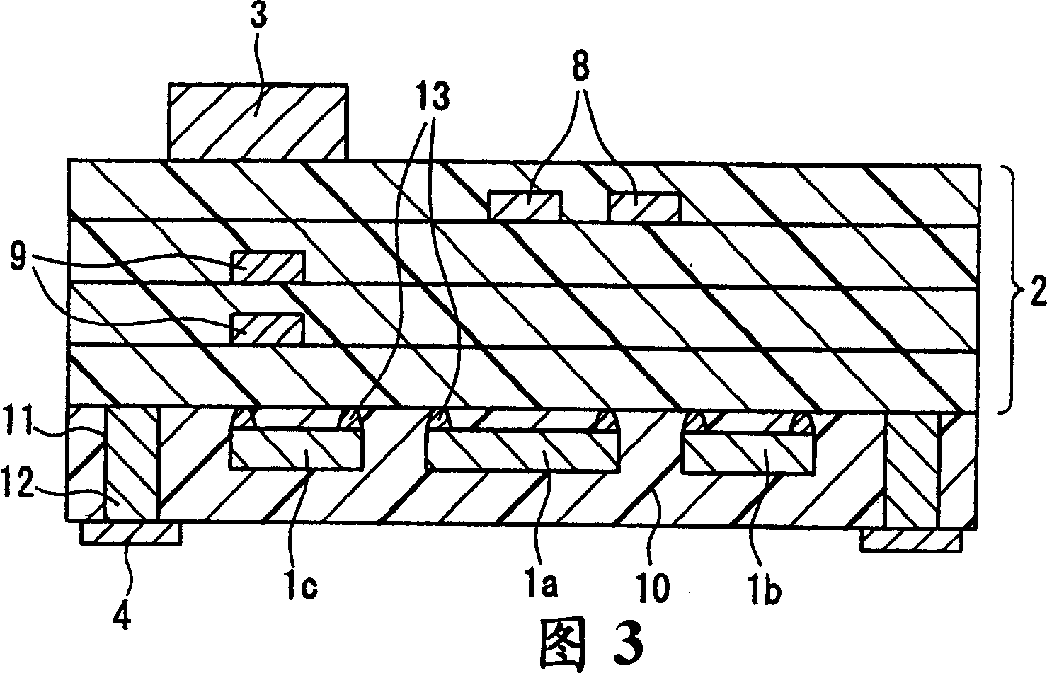
[0045] Referring now to the sectional view of the high-frequency semiconductor device shown in Figure 3, the second aspect of the present invention

[0046] Examples will be described.

[0047] The device in Figure 3 follows the figure 1 The first embodiment shown differs in that the gallium arsenide power semiconductor element 1a, the gallium arsenide semiconductor element 1b and the silicon semiconductor element 1c are bonded to the ceramic multilayer substrate 2 via bumps 13 whose cores are metallic. The circuit pattern on the bottom is connected by flip-chip.

[0048] On the bump 13, the SBB (Stand Ball Bonding) method of gold wire is used, and the gap between the semiconductor elements 1a, 1b, 1c and the ceramic multilayer substrate 2 is about 40 μm. Other methods for providing the bump 13 include: a method of plating around the copper core material and connecting it with a conductive resin; a method of using ACF (Anisotropic Conductive Film); and a method of using sold...

no. 3 example

[0052] Referring now to the cross-sectional view of the high-frequency semiconductor device shown in FIG. 4 and Figure 5 The shown perspective view of the high-frequency semiconductor device of FIG. 4, viewed from the rear, illustrates a third embodiment of the present invention.

[0053] The device in Fig. 4 is different from the second embodiment shown in Fig. 3 in that: directly below the gallium arsenide power semiconductor element 1a as the power amplifier, an interlayer connection structure via hole 21 is formed; The lower surface of 10 is formed with electrodes 14 for heat dissipation, and its position is consistent with the through holes 21 of the interlayer connection structure. Such as Figure 5 As shown, on the lower surface of the composite resin material layer 10, a plurality of electrodes 4 for external connection and electrodes 14 for heat dissipation having a larger area than the electrodes 4 for external connection are formed. In this way, through the throu...


PUM

PropertyMeasurementUnit
thermal conductivityaaaaaaaaaa
diameteraaaaaaaaaa

Abstract

The invention relates to a high-frequency semiconductor device comprising a ceramic substrate (2); an element group (1a,1b,1c) including semiconductor elements and passive components mounted onto a bottom portion of the ceramic substrate (2); and a composite resin material layer formed on the bottom portion of the ceramic substrate so as to bury the element group; wherein the composite resin material layer(10) is formed by a composite resin material including an epoxy resin and an inorganic filler material, and the composite resin material layer has a flat bottom surface on which electrodes (4) for connecting to the outside are formed.

Description

technical field [0001] The present invention relates to the structure of a high-frequency semiconductor device equipped with a high-frequency semiconductor element, an integrated circuit element for control and its peripheral circuit, and specifically relates to a packaging structure. technical background [0002] It is increasingly desired to adopt an all-in-one structure that integrates a receiving system and a transmitting system, and realize modularization by using high-frequency semiconductor devices mainly used in mobile communication equipment such as cellular phones as radio frequency modules. At the same time, by loading high-frequency semiconductor components, integrated circuit components for control and their peripheral circuits, and incorporating them into a system that integrates the receiving system and the transmitting system, we will strive to increase the number of actually loaded semiconductor components and chip components. The miniaturization of packages...

Claims


Application Information

Patent Timeline
Patent Type & Authority Applications(China)
IPC IPC(8): H01L23/29H01L23/31H01L23/538H01L23/66H01L25/04H01L25/18H05K1/03H05K1/11H05K1/18H05K3/28H05K3/46
CPCH01L2924/09701H05K1/183H01L23/3121H01L23/66H01L2924/12041H01L2924/19105H01L2224/16H01L2224/48091H05K3/4614H01L2224/16225H05K1/112H01L2924/3025H01L2924/01078H01L24/48H01L2924/3011H01L2924/19041H01L23/5389H01L2924/01079H05K3/4629H05K3/284H01L2924/01057H01L2224/45144H05K1/0306H01L2924/16152H05K1/186H01L2924/01019H01L2224/48227H01L2924/14H01L2924/00014H01L24/45H01L2924/181H01L2924/00015H01L2924/00H01L2224/45015H01L2924/207
Inventor 竹原秀树吉川则之金泽邦彦中谷诚一
Owner PANASONIC CORP
Why Eureka
Try Eureka