Manufacture of non-volatile memory

A non-volatile, manufacturing method technology, applied in semiconductor/solid-state device manufacturing, electrical components, circuits, etc., can solve problems such as interference, affecting normal operation, serious problems, etc., to achieve interference reduction, gate line width reduction, The effect of increasing distance

Inactive Publication Date: 2003-06-04
MACRONIX INT CO LTD
View PDF0 Cites 13 Cited by
  • Summary
  • Abstract
  • Description
  • Claims
  • Application Information

AI Technical Summary

Problems solved by technology

[0005] Although in the above known technology, the data storage areas 170 and 180 can be programmed or erased respectively, the charge stored in the data storage area 170 (180) will interfere with the data storage area 180 (170), affect its normal operation
Furthermore, when the device size (gate line width) is reduced, the distance between the two data storage regions 170 and 180 is also reduced, which makes the interference phenomenon more serious, so the reduction of the device is difficult to achieve

Method used


Image

  • Manufacture of non-volatile memory
  • Manufacture of non-volatile memory
  • Manufacture of non-volatile memory

Examples


Embodiment Construction

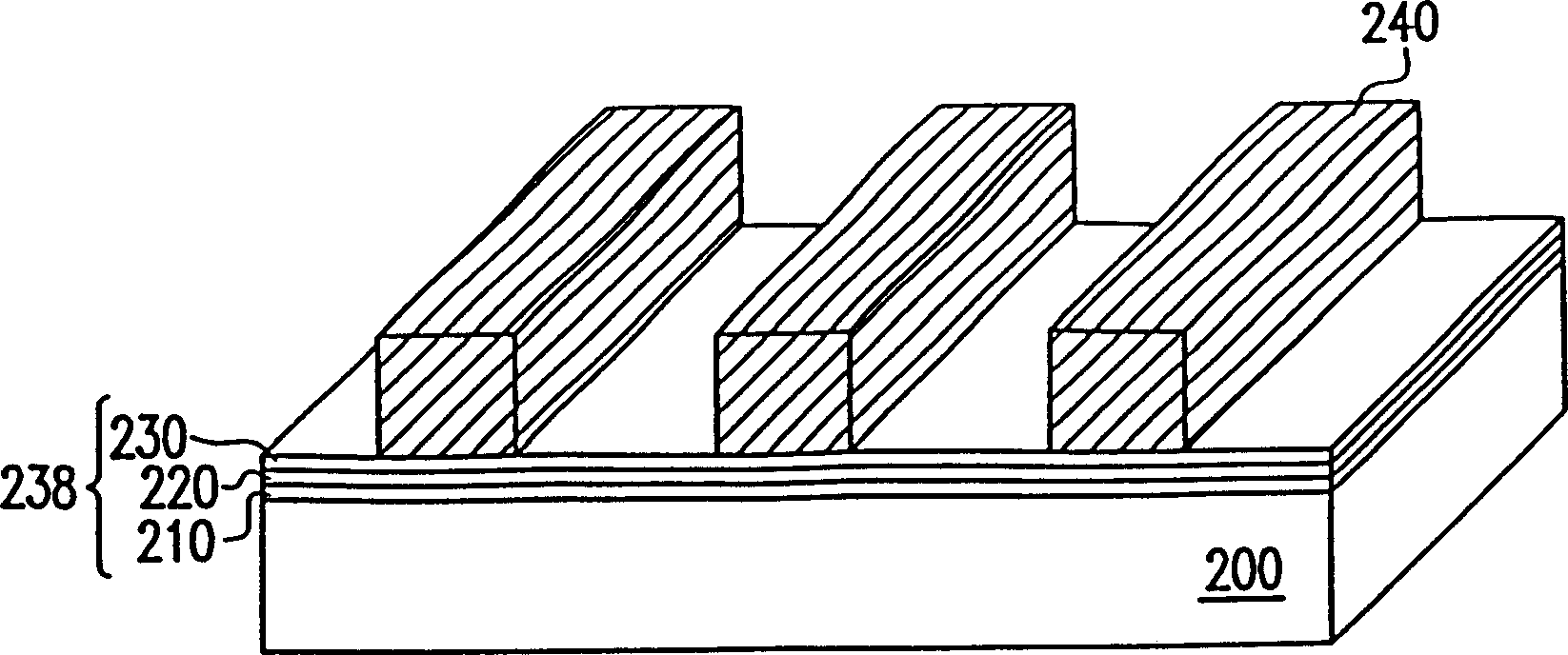
[0022] This preferred embodiment takes the manufacturing process of SONOS memory as an example, and uses Figure 2A ~ Figure 2E As an aid, the method of manufacturing the nonvolatile memory of the present invention will be described.

[0023] Please refer to Figure 2A First, a substrate 200 is provided, and then a silicon oxide layer 210 , a silicon nitride layer 220 , and a silicon oxide layer 230 are sequentially formed on the substrate 200 , and these three are collectively referred to as a charge trap layer 238 . Among them, the formation method of the silicon oxide layer 210 is preferably Thermal Oxidation, the formation method of the silicon nitride layer 220 is, for example, low-pressure chemical vapor deposition (LPCVD), and the formation method of the silicon oxide layer 230 is, for example, nitrogen oxide the surface of silicon oxide layer 220. Next, a strip-shaped conductive layer 240 parallel to each other is formed on the substrate 200 , which is the precursor ...


PUM


Abstract

The manufacture of non-volatile memory includes forming charge trap layer of insulating material and conducting strips as precursor of grid on the substrate; forming embedded bit lines between conducting strips with some interval being maintained between the embedded bit line and the adjacent conducting strips; forming high-dielectric constant interval walls on the side walls of the conducting strips; defining the conducting strips to form grids and finally forming electrically connecting word lines over the substrate. The high-dielectric constant interval walls is of material with sufficienthigh dielectric constant and has enough width, so that the channel formed by the non-volatile memory can extend to below the high-dielectric constant interval walls and form electric connection with the embedded bit lines.

Description

technical field [0001] The present invention relates to a manufacturing method of a semiconductor device, and in particular to a manufacturing method of a non-volatile memory (Non-volatile Memory, NVM). Background technique [0002] Non-volatile memory can still retain the data in it when the power is turned off, and has the advantages of being light, thin, short, and small, so its application is becoming more and more extensive. Early non-volatile memories used polysilicon floating gate (Floating Gate) to store data (charge). Since polysilicon is a conductor, the charge will be dispersed throughout the polysilicon floating gate, so that only one bit of data can be stored in a memory cell. . The most recently proposed non-volatile memory is the silicon nitride read-only memory ( N itride ROM , NROM) and SONOS ( S ubstrate- O xide- N itride- O xide- S Silicon) memory and the like, a non-volatile memory that uses a silicon nitride layer as a charge storage layer. Sinc...

Claims


Application Information

Patent Timeline
Patent Type & Authority Applications(China)
IPC IPC(8): H01L21/8239H01L21/8246
Inventor 林宏穗赖汉昭卢道政
Owner MACRONIX INT CO LTD
Why Eureka
Try Eureka