Organic film transistor

An organic thin film and organic film technology, applied in the field of organic TFT, can solve the problems of insufficient mobility of organic compounds and inability to achieve driving speed, etc., and achieve the effects of high-speed response, short channel length, and high carrier mobility

Inactive Publication Date: 2003-07-30
NEC CORP
View PDF2 Cites 8 Cited by
  • Summary
  • Abstract
  • Description
  • Claims
  • Application Information

AI Technical Summary

Problems solved by technology

However, also in this case, since the mobility of the organic compound is insufficient, a sufficient driving speed cannot be achieved

Method used


Image

  • Organic film transistor
  • Organic film transistor
  • Organic film transistor

Examples


no. 1 approach

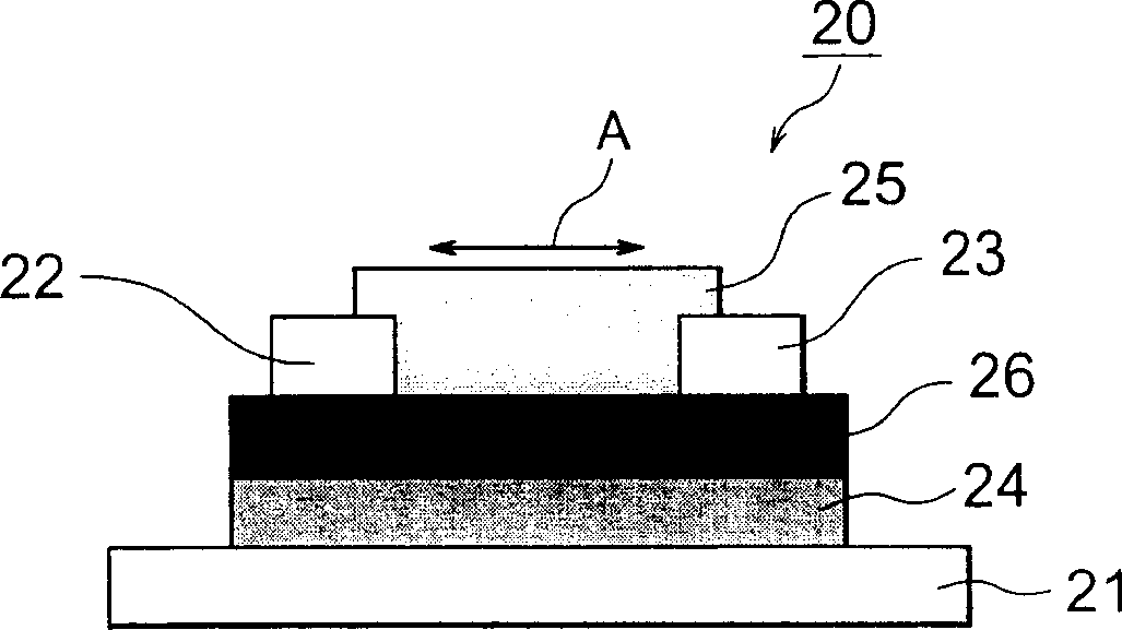
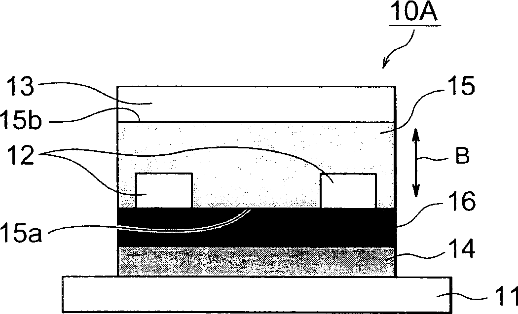
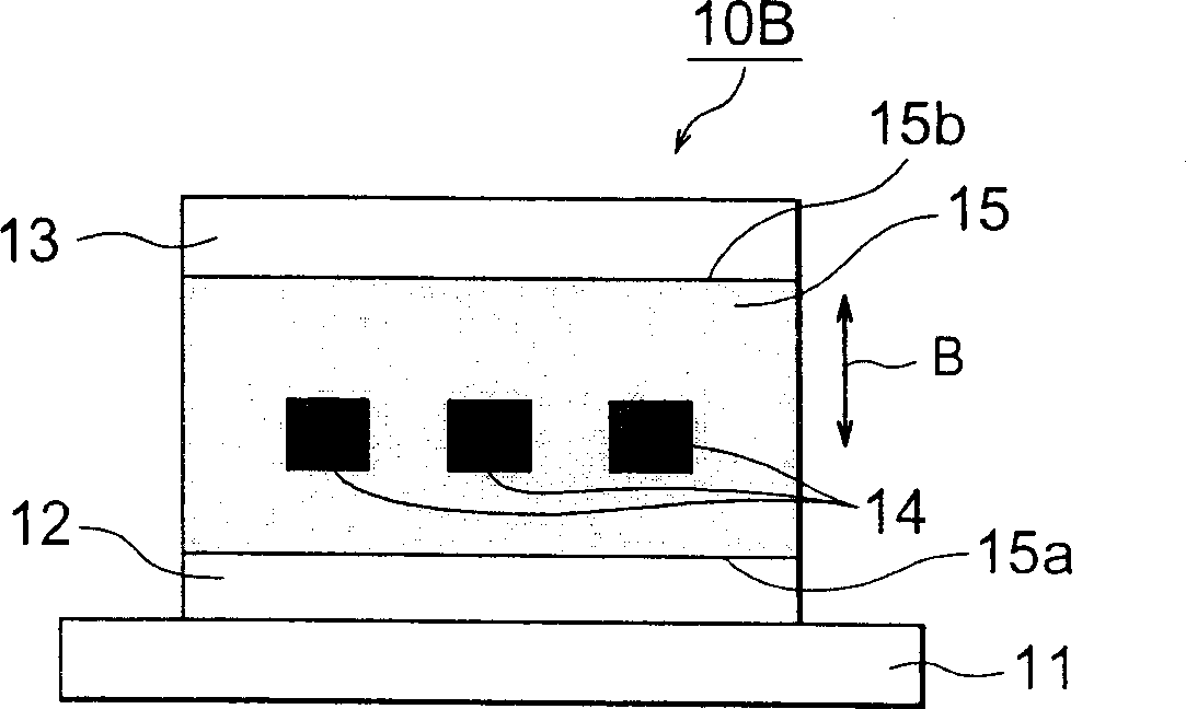
[0024] Such as figure 2 As shown, an organic TFT 10A having a FET (Field Effect Transistor) structure includes a laminated structure on a substrate 11 . The laminated structure includes a structure on a substrate 11 in which gate electrodes 14 and dielectric layers 16 are arranged in sequence, and strip-shaped source electrodes (first electrodes) 12 are installed on the dielectric layers 16 respectively. Further, an organic film (organic compound layer) 15 is formed on the surface of the source electrode 12 and the exposed surface of the dielectric layer 16 , and a drain electrode (second electrode) 13 is formed on the organic film 15 . The source electrode 12 is in contact with the side and bottom surfaces of the organic film 15 , and the drain electrode 13 is in contact with the top surface 15 b of the organic film 15 .

[0025] In the organic TFT 10A having the above structure, the organic film 15 forms a channel region, and the ON / OFF operation controls the flow of curre...

Embodiment 1

[0062] exist figure 2 The organic TFT 10A of the first embodiment shown in is manufactured as follows.

[0063] On the substrate 11, a gate electrode 14 was formed to a thickness of 100 nm by vacuum-depositing chromium. Then, SiO is formed on the gate electrode 14 by sputtering 2 film, thereby forming a dielectric layer 16 with a thickness of 300 nm. A magnesium-silver alloy is vacuum-deposited on the dielectric layer 16 through a metal mask to form a strip-shaped source electrode 12 with a thickness of 100 nm.

[0064] Then, compound (1') was vacuum-deposited on the dielectric layer 16 and the source electrode 12 to form an organic film 15 with a thickness of 300 nm. Next, a magnesium-silver alloy was vacuum-deposited on the organic film 15 to form the drain electrode 13 with a thickness of 200 nm, thereby fabricating the organic TFT 10A.

[0065] A rectangular pulse voltage with a frequency of 1k Hz and a maximum voltage of 8.5V was applied to the gate electrode 14 of t...

Embodiment 2

[0067] An organic TFT was fabricated according to the procedure of Example 1, except that compound (3') was used instead of compound (1'). The response rise time for measuring the conduction state between the source-drain electrodes of the organic TFT is less than 1 μs, which is similar to that of Embodiment 1.


PUM


Abstract

An organic TFT including an organic film, first and second electrodes each disposed in contact with opposite surfaces of the organic film each other; and a third electrode disposed at a specified distance from each of the first and second electrodes, the third electrode being applied with a voltage to control current flowing from one of the first and the second electrodes to the other through the organic film; and the organic film including a compound represented by general formula [1]. In this TFT, the carrier moves from one of the first and the second electrodes to the other in the direction of the film thickness of the organic film. The device structure realizes the enough short channel length. The organic film provides the higher mobility, thereby the organic TFT with the sufficiently higher speed response is realized.

Description

technical field [0001] The present invention relates to organic thin film transistors (TFTs) having organic semiconductor layers (organic films), and more particularly, to organic TFTs operating at higher speeds and higher frequencies. Background technique [0002] TFTs are widely used as switching devices for display devices such as LCDs. Conventional TFTs are made of amorphous or polycrystalline silicon. A CVD apparatus for manufacturing TFTs is expensive, and manufacturing large-sized displays with TFTs is accompanied by a significant increase in manufacturing costs. Since film formation of amorphous or polycrystalline silicon is performed at relatively high temperature, some kinds of substrates, such as resin substrates, cannot be used in TFTs or exclude light-weight resin substrates. [0003] TFTs using organic compounds instead of amorphous or polycrystalline silicon have been proposed to overcome the above problems. Vacuum deposition techniques and coating techniqu...

Claims


Application Information

Patent Timeline
Patent Type & Authority Applications(China)
IPC IPC(8): H01L51/05H01L27/01H01L29/786H01L29/80H01L51/00H01L51/30
CPCH01L51/005H01L51/0059H01L51/0077H01L51/0052H01L51/057H01L51/0081H01L51/0516H01L51/0094H10K85/60H10K85/615H10K85/631H10K85/30H10K85/324H10K10/468H10K85/40H10K10/491
Inventor 东口达小田敦石川仁志
Owner NEC CORP
Why Eureka
Try Eureka