Method for removing residual polycrystalline silicon

A technology of polysilicon and polysilicon layer, applied in the direction of electrical components, semiconductor/solid-state device manufacturing, circuits, etc., can solve problems such as electrical short circuit, achieve the effect of reducing thermal budget and avoiding erosion

Inactive Publication Date: 2003-08-06
MACRONIX INT CO LTD
View PDF0 Cites 7 Cited by
  • Summary
  • Abstract
  • Description
  • Claims
  • Application Information

AI Technical Summary

Problems solved by technology

Therefore, the present invention provides a method for removing polysilicon residues, which can convert polysili

Method used


Image

  • Method for removing residual polycrystalline silicon
  • Method for removing residual polycrystalline silicon
  • Method for removing residual polycrystalline silicon

Examples


Embodiment Construction

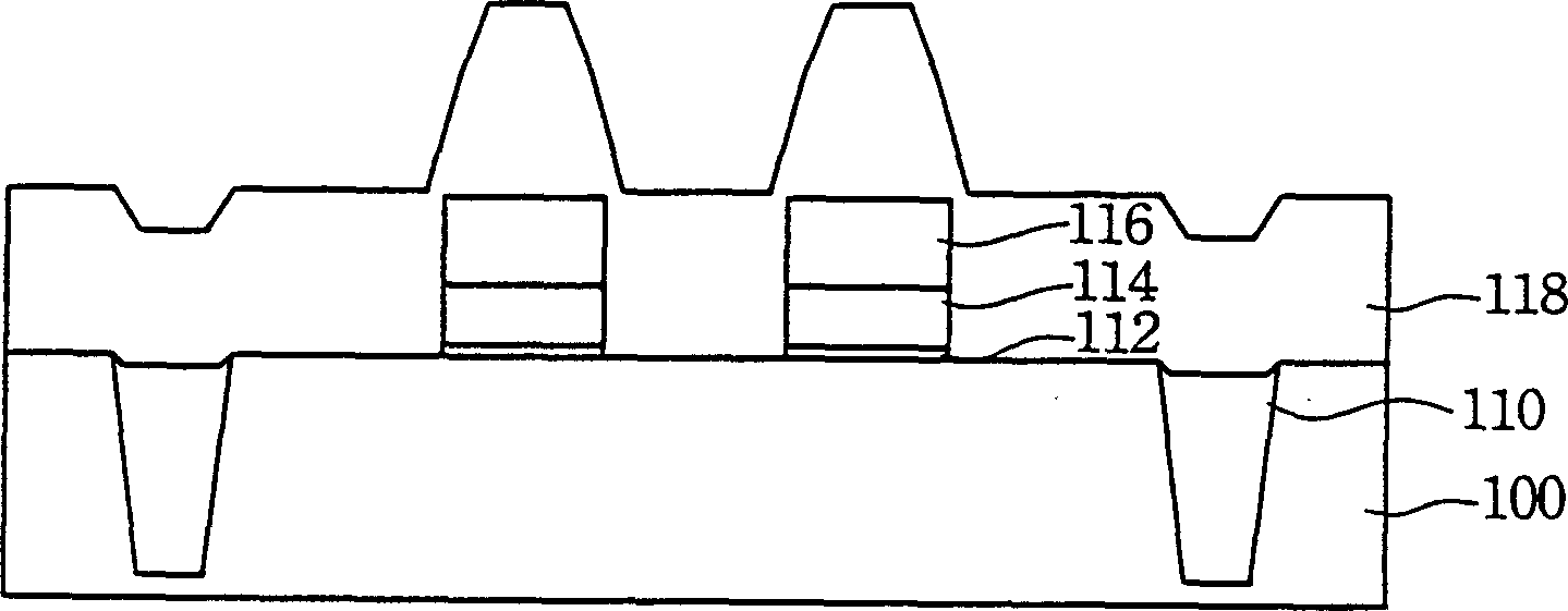
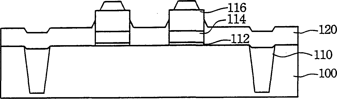
[0028] The invention provides a method for removing polysilicon residues, which can effectively remove the polysilicon residues on the side walls, convert the residual polysilicons into silicon dioxide, and avoid the corrosion problem caused by excessive oxidation.

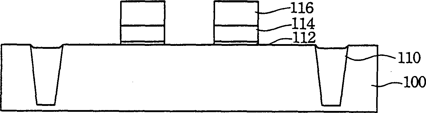
[0029] Figures 1A-1I It is a schematic cross-sectional view illustrating the process of the flash memory cell of the present invention. Please refer to Figure 1A Firstly, a semiconductor substrate 100 is provided, such as a P-type silicon substrate having a lattice arrangement. Next, an isolation structure 110 is fabricated in the substrate 100, and an active region of each memory cell is planned. The isolation structure 110 is, for example, a field oxide layer formed by local oxidation of silicon (LOCOS), and is preferably a shallow trench Isolated (STI) structure.

[0030] Next, a gate oxide layer 112 , a first polysilicon layer 114 and a silicon nitride layer 116 are sequentially formed on the substrate 10...


PUM


Abstract

A method for removing residual of polycrystalline silicond is first of all to insert oxygen ions in polysilicon remains with tilt ionic inserting method in which the residual area fuel of oxygen ionsand convert to SiO2 completely by oxygen an nealing to reduce conductivity of the polysilicon and oxygen erosion will not occur which not only eliminate polysilicon remain but also avoid the erosion resulted in over oxidation by tilt oxygen ion insertion to recuce heat predict and reach the aim of converting to converting to SiO2 completely.

Description

technical field [0001] The present invention relates to a manufacturing method of a semiconductor memory, and in particular to a method for removing polysilicon (polysilicon) residue between word lines. Background technique [0002] As computer microprocessors become faster and faster, the amount of data calculations performed by computer software will become larger, and the demand for natural memory will also be higher. Random access memory (RAM) components have long been widely used in computers, but their data will be erased as the power supply is interrupted, so it is also called volatile memory; another component called non-volatile memory is Because its data will not disappear due to the interruption of power supply, it can be used in other different occasions, such as mask read-only memory (Mask ROM), erasable programmable read-only memory (EPROM), electrically erasable programmable Read memory (EEPROM), etc. [0003] In addition, there is a non-volatile memory call...

Claims


Application Information

Patent Timeline
IPC IPC(8): H01L21/265H01L21/324H01L21/8239
Inventor 苏俊联王俊淇陈铭祥
Owner MACRONIX INT CO LTD
Why Eureka
Try Eureka