
Method for preparing neodymium doped yttrium vanadate crystal waveguide laser by ion implantation

A technology of ion implantation and yttrium vanadate, which is applied in lasers, phonon exciters, laser components, etc., can solve problems such as limited scope of application and impact

Inactive Publication Date: 2003-08-06
SHANDONG UNIV
View PDF0 Cites 6 Cited by
  • Summary
  • Abstract
  • Description
  • Claims
  • Application Information

AI Technical Summary

Problems solved by technology

Their main disadvantage is that the prepared waveguide has a relatively large impact on the original crystal properties, and the scope of application is limited. At present, it can only be used in certain crystals suitable for exchange or diffusion (such as LiNbO 3 ) to achieve waveguide lasers, and for such as Nd: YVO 4 For many crystals such as ion exchange or diffusion, etc. cannot be achieved

Method used


Image

  • Method for preparing neodymium doped yttrium vanadate crystal waveguide laser by ion implantation
  • Method for preparing neodymium doped yttrium vanadate crystal waveguide laser by ion implantation
  • Method for preparing neodymium doped yttrium vanadate crystal waveguide laser by ion implantation

Examples


Embodiment 1

[0015] (5) Specific implementation methods Example 1: Preparation of planar waveguide laser for phosphorus ion implantation of neodymium-doped yttrium vanadate crystal

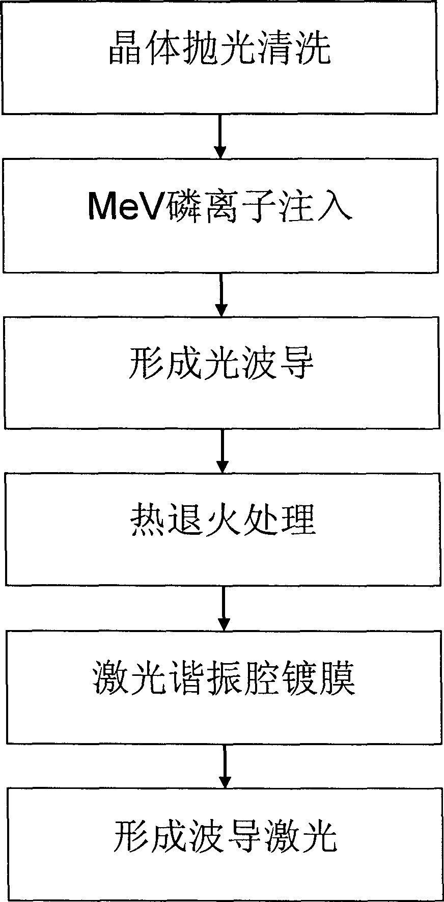
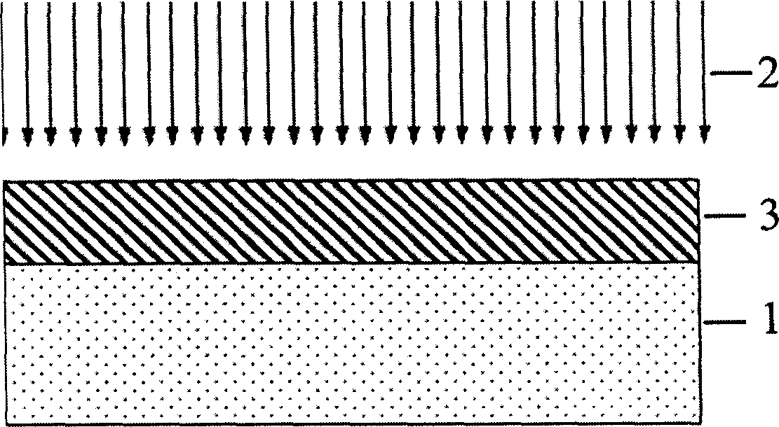
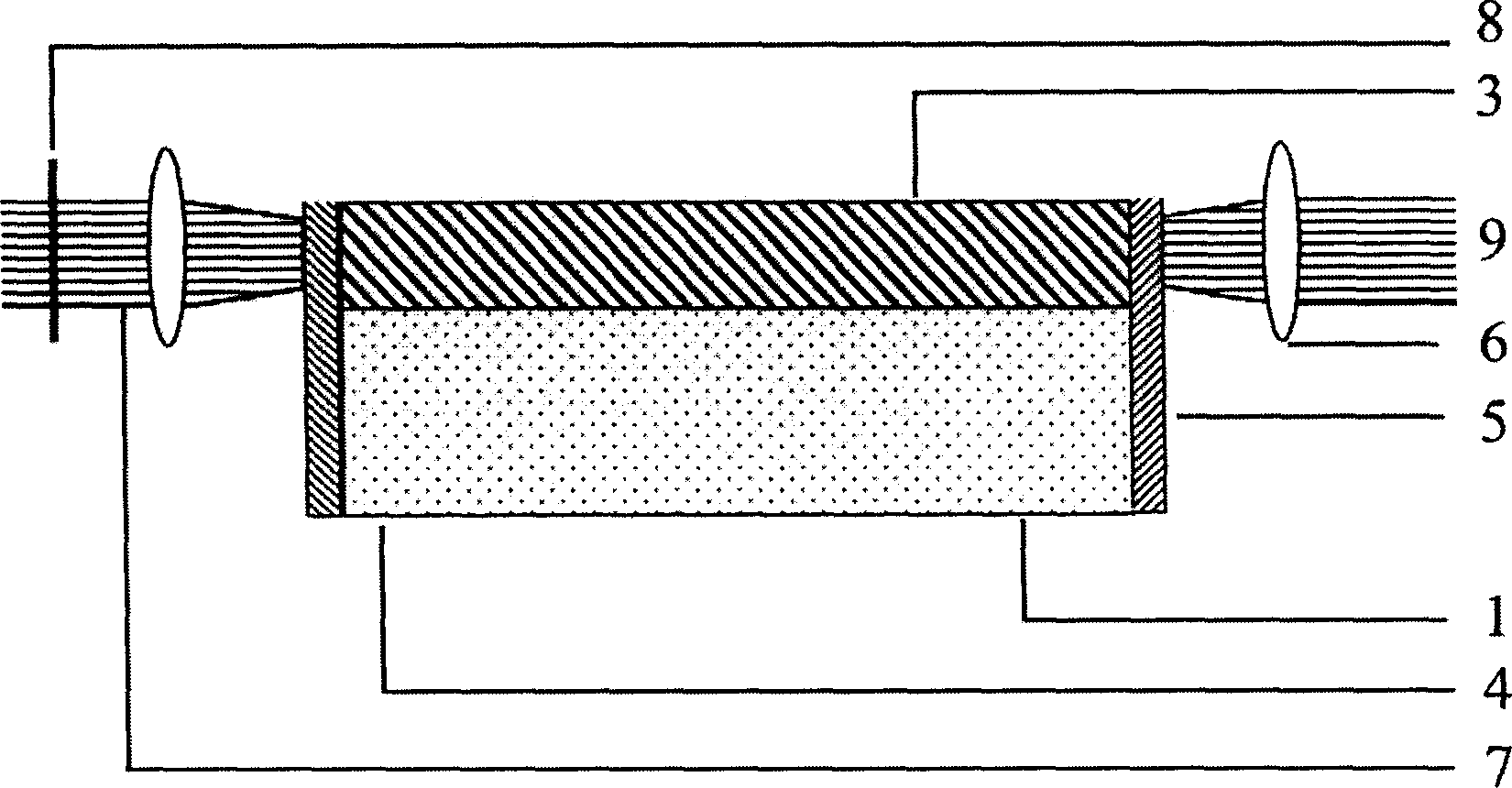
[0016] Planar waveguide production process: Nd cut by x 3+ : YVO 4 A crystal sample (1) with a size of 5mm×5mm×2mm. The surface (5mm×5mm) is polished, and the two surfaces (5mm×2mm) perpendicular to the y direction are also polished. MeV phosphorus ion implantation (2): implantation energy is 2.8MeV, dose is 1×10 14 ions / cm² P + ions, the surface forms a refractive index-increased optical waveguide (3) with a thickness of 2.2 microns. The sample was placed in air for thermal annealing at 260°C for 60 minutes.

[0017] Coating on the end face of the waveguide: The two end faces of the waveguide (5mm×2mm) need to be coated: the coating on the input end of the laser resonator (4) and the output end of the laser resonator (5), which need to be able to cover the range of the end face waveguide. 808nm fully tr...

Embodiment 2

[0018] Output of the waveguide laser: use a semiconductor laser to generate pump light (7) with a wavelength of 808nm, and the laser output from the laser is modulated by a polarizer (8) to become TM polarized light, which is transformed into parallel light by a collimator, and then passed through a microscope objective lens (6) Coupling into Nd 3+ : YVO 4 The waveguide layer of the crystal is pumped, Nd 3+ : YVO 4 The waveguide layer of the crystal can generate laser light with a wavelength of 1064nm, which can be coupled out by the objective lens (6) to output waveguide laser light (9) of 1064nm. Example 2 Preparation of strip waveguide laser by implanting phosphorous ions into neodymium-doped yttrium vanadate crystal

[0019] The production process of the strip optical waveguide: a piece of Nd cut by x 3+ : YVO 4 Sample (1), the size is 5mm×5mm×2mm. The surface (5mm×5mm) is polished, and the two surfaces (5mm×2mm) perpendicular to the y direction are also polished. A...


PUM


Abstract

This invention relates to a method for preparation of crystal waveguide laser with ion implantation, mainly forming a plane and strip waveguide in Nd:YVO4 crystal and strip waveguide laser output, applying P ion implantation with energy power of 2.0-6.0 Mev, dose of 1X10 to the power 12 - 5X10 to the power 15 ions / cm2 to form plane light waveguide on Nd3+: YVO4 crystal surface or form a strip mask first, then to proceed with P ion implantation to form the Nd3+: YVO4 strip light waveguide to pump the plane or strip waveguide with a certain wavelength and power laser, to output infrared laser with the wavelength of about 1064nm after laser cavity coating to its end face.

Description

(1) Technical field [0001] The invention relates to a method for preparing crystal waveguide lasers, especially suitable for the preparation of plane and strip waveguide lasers of neodymium ion-doped yttrium vanadate crystals. The invention belongs to a waveguide preparation method in the field of optoelectronic devices. (2) Background technology [0002] Neodymium ion-doped yttrium vanadate (Nd 3+ : YVO 4 ) crystal is a widely used laser crystal, which can generate laser light with a wavelength of 1064 nanometers (nm), and has important applications in optical communications. [0003] Optical waveguide is the basic element of integrated optics, which is defined as a micron-scale high-refractive-index medium area surrounded by low-refractive-index medium. Due to the total internal reflection of the light beam on the side of the low-refractive-index medium at the medium boundary, it is confined to propagate in the high-refractive-index medium. Optical waveguides can confi...

Claims


Application Information

Patent Timeline
Patent Type & Authority Applications(China)
IPC IPC(8): H01S3/063H01S3/16
Inventor 陈峰王雪林王克明卢霏胡卉
Owner SHANDONG UNIV
Learn More