GaN-based semiconductor device and manufacturing method thereof

A manufacturing method and semiconductor technology, applied in the direction of semiconductor devices, semiconductor lasers, laser components, etc., can solve the problems of large dislocation density, silicon and GaN lattice mismatch, etc., to reduce the dislocation density and reduce the cost of epitaxy , the effect of reducing light loss

Active Publication Date: 2017-05-17
SUZHOU INST OF NANO TECH & NANO BIONICS CHINESE ACEDEMY OF SCI
View PDF3 Cites 10 Cited by
  • Summary
  • Abstract
  • Description
  • Claims
  • Application Information

AI Technical Summary

Problems solved by technology

However, there are still great challenges in using silicon substrates, mainly due to the large lattice mismatch between silicon and GaN, which is prone to generate large dislocation densities

Method used


Image

  • GaN-based semiconductor device and manufacturing method thereof
  • GaN-based semiconductor device and manufacturing method thereof
  • GaN-based semiconductor device and manufacturing method thereof

Examples


Embodiment 1

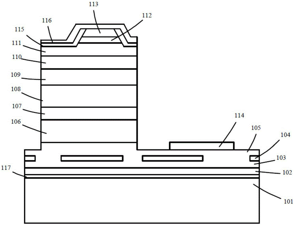
[0038] Refer to Example 1 figure 1 , This embodiment 1 provides a GaN-based violet superluminescent light emitting diode grown on a silicon substrate 101, the emission wavelength is 405 nm, and the material is grown by using the tightly coupled vertical reaction chamber MOCVD growth system of Aixtron Corporation. Its specific preparation method is as follows:

[0039] a. In a hydrogen atmosphere, at a temperature of 1290 °C, TMAl was introduced as a group III source, NH 3 As the V group source, grow an AlN buffer layer 117 with a thickness of 300 nm; then pass in TMGa to grow a layer of Al with a thickness of 300 nm 0.1 Ga 0.9 N buffer layer 102; grow another GaN template layer 103 with a thickness of 3 μm; use PECVD method to deposit 7 cycles of SiO on the GaN layer 2 / SiN x The composite dielectric layer 104, the lower layer is SiO 2 , the thickness is 75nm, the upper layer is SiN x , the thickness is 53nm, and then the window area is etched by photolithography, the wi...

Embodiment 2

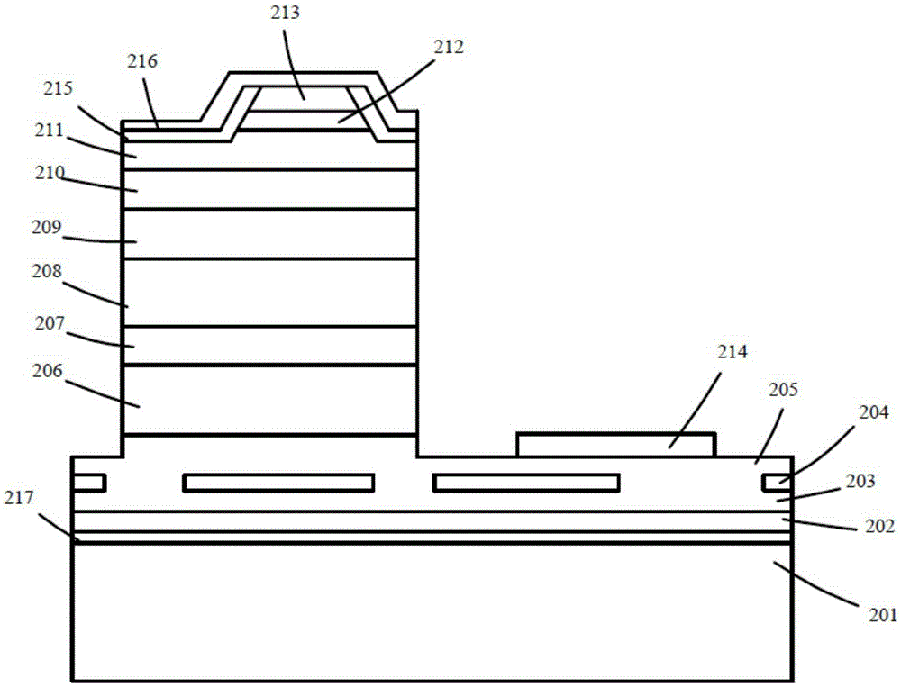
[0049] Refer to Example 2 figure 2 , this embodiment 2 provides a GaN-based blue light laser grown on a silicon substrate 201, using lateral epitaxial growth of a GaN buffer layer, in which three cycles of SiO are grown 2 / SiN x The mask layer is used as a light reflection layer, and its emission wavelength is 440 nm, and the material is grown by the tightly coupled vertical reaction chamber MOCVD growth system of Aixtron Company. Its specific preparation method is as follows:

[0050] a. In a hydrogen atmosphere, at a temperature of 1290 °C, TMAl was introduced as a group III source, NH 3 As the V group source, grow an AlN buffer layer 217 with a thickness of 300 nm; then pass in TMGa to grow a layer of Al with a thickness of 300 nm 0.1 Ga 0.9 N buffer layer 202; bonding image 3 As shown, a GaN template layer 203 with a thickness of 3 μm is grown again; 7 cycles of SiO are deposited on the GaN layer by PECVD method 2 / SiN x The composite dielectric layer 204, the low...

Embodiment 3

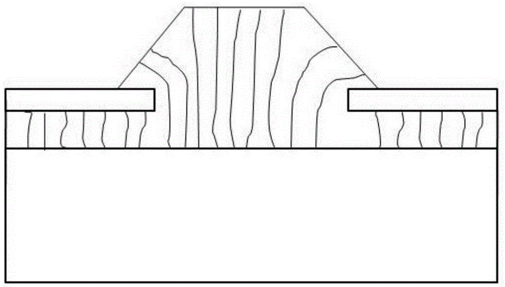
[0061] Example 3 see Figure 5 , this embodiment 3 provides a GaN-based blue light laser grown on a silicon substrate 301, using lateral epitaxial growth of a GaN buffer layer, in which a layer of SiO is grown 2 / SiN x The dielectric mask layer is used as the interface layer to form a flat-plate coupled optical waveguide laser with an emission wavelength of 440 nm. Material growth was performed using a tightly coupled vertical chamber MOCVD growth system from Aixtron Corporation. Its specific preparation method is as follows:

[0062] a. In a hydrogen atmosphere, at a temperature of 1290 °C, TMAl was introduced as a group III source, NH 3 As the V group source, grow an AlN buffer layer 302 with a thickness of 300 nm; then pass in TMGa to grow a layer of Al with a thickness of 300 nm 0.1 Ga 0.9 N buffer layer 303; grow another GaN template layer 304 with a thickness of 3 μm; use PECVD method to deposit SiO on the GaN layer 2 / SiN x Composite dielectric layer 305, the low...


PUM

PropertyMeasurementUnit
thicknessaaaaaaaaaa
thicknessaaaaaaaaaa
thicknessaaaaaaaaaa

Abstract

The invention discloses a GaN-based semiconductor device and a manufacturing method thereof. The GaN-based semiconductor device comprises a silicon substrate and an epitaxial layer formed on the silicon substrate, and is characterized in that the epitaxial layer comprises an AlN nucleating layer, an AlGaN buffer layer and a GaN buffer layer which are sequentially formed on the silicon substrate. According to the invention, a dielectric film is adopted to act as a mask layer, different effects are achieved through regulating and controlling the periodicity of a dielectric layer, and the dielectric layer can act as a limiting layer when the periodicity reaches the maximum, so that the optical loss can be effectively reduced, and threshold current of a laser and a super-radiation light-emitting diode is reduced; and the electric layer acts as an interface layer when the periodicity is small and forms another optical waveguide structure together with AlGaN at the bottom, a planar coupling optical waveguide laser and a super-radiation light-emitting diode are formed, and a nearly-circular light spot with a good shape can be acquired.

Description

technical field [0001] The invention belongs to the technical field of semiconductor optoelectronics, and in particular relates to a GaN-based semiconductor device such as a laser, a super-radiant light-emitting diode, and a manufacturing method thereof. Background technique [0002] Group III nitrides with wurtzite structure are important compound semiconductor materials and have great application prospects in optoelectronics and microelectronics. In recent years, they have been highly valued by researchers and developed rapidly. Due to the wide energy band of the gallium nitride material system, by adjusting the compound composition, the wavelength of GaN-based light-emitting devices can cover a wide range from infrared to visible light to ultraviolet, which is the current realization of blue and violet lasers and superluminescence. The best choice for diodes. [0003] Internationally, blue and violet lasers based on gallium nitride substrates have been produced, but the ...

Claims


Application Information

Patent Timeline
Patent Type & Authority Applications(China)
IPC IPC(8): H01L33/00H01S5/343
CPCH01L33/0045H01L33/007H01S5/34333
Inventor 严威孙逸冯美鑫周宇孙钱杨辉
Owner SUZHOU INST OF NANO TECH & NANO BIONICS CHINESE ACEDEMY OF SCI
Why Eureka
Try Eureka