Pellet electrical resistor and producing method thereof
A resistor and chip technology, applied in the manufacture of resistors, resistors, thick film resistors, etc., can solve the problems of small resistors, difficult to obtain, etc., and achieve the effect of low TCR, good heat resistance, and small resistance
- Summary
- Abstract
- Description
- Claims
- Application Information
AI Technical Summary
Problems solved by technology
Method used
Image

Examples
Embodiment 1
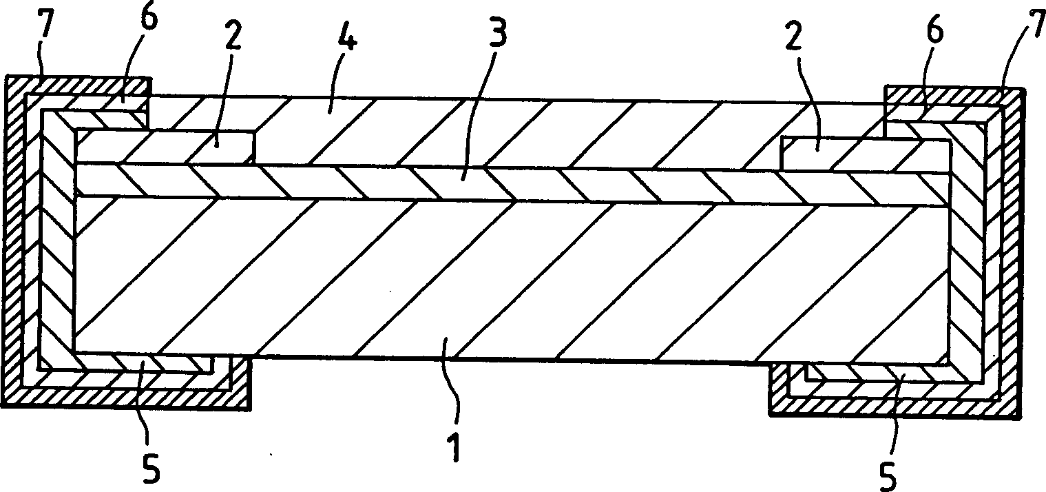
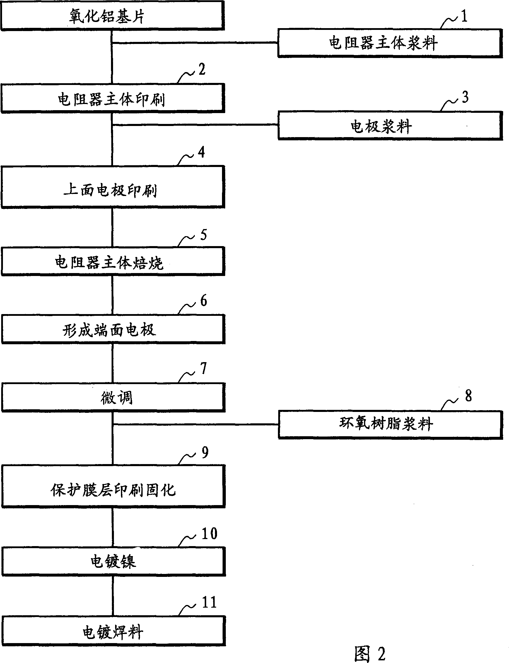
[0034] figure 1 is a sectional view of the chip resistor of the first embodiment of the present invention. In this figure, 3 denotes a resistive layer. Using a resistor body paste having an alloy composition shown in Table 1 below, a resistor layer was printed on one face of a square insulating substrate (hereinafter simply referred to as a substrate) 1 by a thick film technique such as screen printing. Next, in the same manner as the resistive layer 3, the upper electrode layer 2 is printed on both ends of the resistive layer 3 opposite to the substrate 1 so as to be in surface contact with the resistive layer 3. In a neutral or reducing atmosphere, the resistance layer 3 and the upper electrode layer 2 are simultaneously fired. Thereafter, protective film 4 is formed covering a part of resistive layer 3 . U-shaped end face electrode layers 5 are formed on both opposite end portions of the substrate 1 and the portion of the resistive layer 3 not covered by the protective ...
Embodiment 2
[0053] The chip resistors obtained by printing and firing the resistor body paste prepared in a similar manner to Example 1 using the alloy powders with the mixing ratios shown in Table 2 will be described below.
[0054] The resistance, temperature coefficient of resistance (TCR), and reliability (high temperature shielding test and thermal shock test) of the thus-prepared chip resistors were measured.
[0055] Comparative examples were prepared in the following manner. Utilize screen plate, on aluminum oxide substrate 10, print the paste that mixes alloy powder, glass frit and organic vehicle liquid to form in the similar manner with embodiment 1, will form on the substrate such as Figure 13 The upper electrode 11 is shown. The paste was dried at 100°C for 10 minutes, and then heated in a nitrogen atmosphere at 1000°C, thereby firing the resistor. Thereafter, end face electrodes and protective films were formed in a similar manner to Example 1, thereby producing a chip re...
Embodiment 3
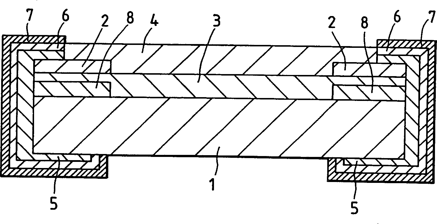
[0060] image 3 is a cross-sectional view of a chip resistor according to a third embodiment of the present invention. In this chip resistor, the lower electrode layer 8 is printed and fired on opposite ends of one side of a square substrate 1, respectively, using a thick film technique such as screen printing. In the lower electrode layer 8, copper or silver powder is used as the metal powder, and a paste in which lead-borosilicate glass is added as a glass frit at a ratio of 3 wt % relative to the metal powder is used. Next, if image 3 As shown, the thick film technology is used to screen-print the resistive body paste with the alloy composition shown in Table 3 below, and the resistive layer 3 is printed on the lower electrode layer 8 . Next, in the same manner as the resistive layer 3, the upper electrode layer 2 is printed on both ends of the resistive layer 3 opposite to the substrate 1 so as to be in surface contact with the resistive layer 3. In a neutral or reduci...
PUM
| Property | Measurement | Unit |
|---|---|---|
| diameter | aaaaa | aaaaa |
| thickness | aaaaa | aaaaa |
| electrical resistance | aaaaa | aaaaa |
Abstract
Description
Claims
Application Information