Semiconductor integrated circuit

An integrated circuit and semiconductor technology, applied in the field of semiconductor integrated circuits, can solve problems such as difficult and reliable laser fusing, and achieve the effects of easy laser fusing, low resistance, and easy laser fusing

Inactive Publication Date: 2004-01-14
MITSUBISHI ELECTRIC CORP
View PDF2 Cites 1 Cited by
  • Summary
  • Abstract
  • Description
  • Claims
  • Application Information

AI Technical Summary

Problems solved by technology

[0011] Therefore, in conventional copper fuses, since most of the laser light irradiated for laser melting is reflected by the copper on the surface of the fuse, it is difficult to reliably perform laser melting as long as a laser with a wavelength in the infrared region is used.

Method used


Image

  • Semiconductor integrated circuit
  • Semiconductor integrated circuit
  • Semiconductor integrated circuit

Examples


Embodiment Construction

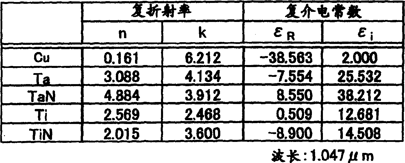
[0056] Since the reflectivity of copper to light in the infrared region is as high as 98% or more (the reflectivity of aluminum in this wavelength region is about 97%), a light absorbing member that effectively absorbs laser light is provided in the present invention. In the embodiment of the present invention, the copper fuse is laser blown using a laser in the infrared region, but the method of the present invention can also be applied to fuses such as aluminum or tungsten.

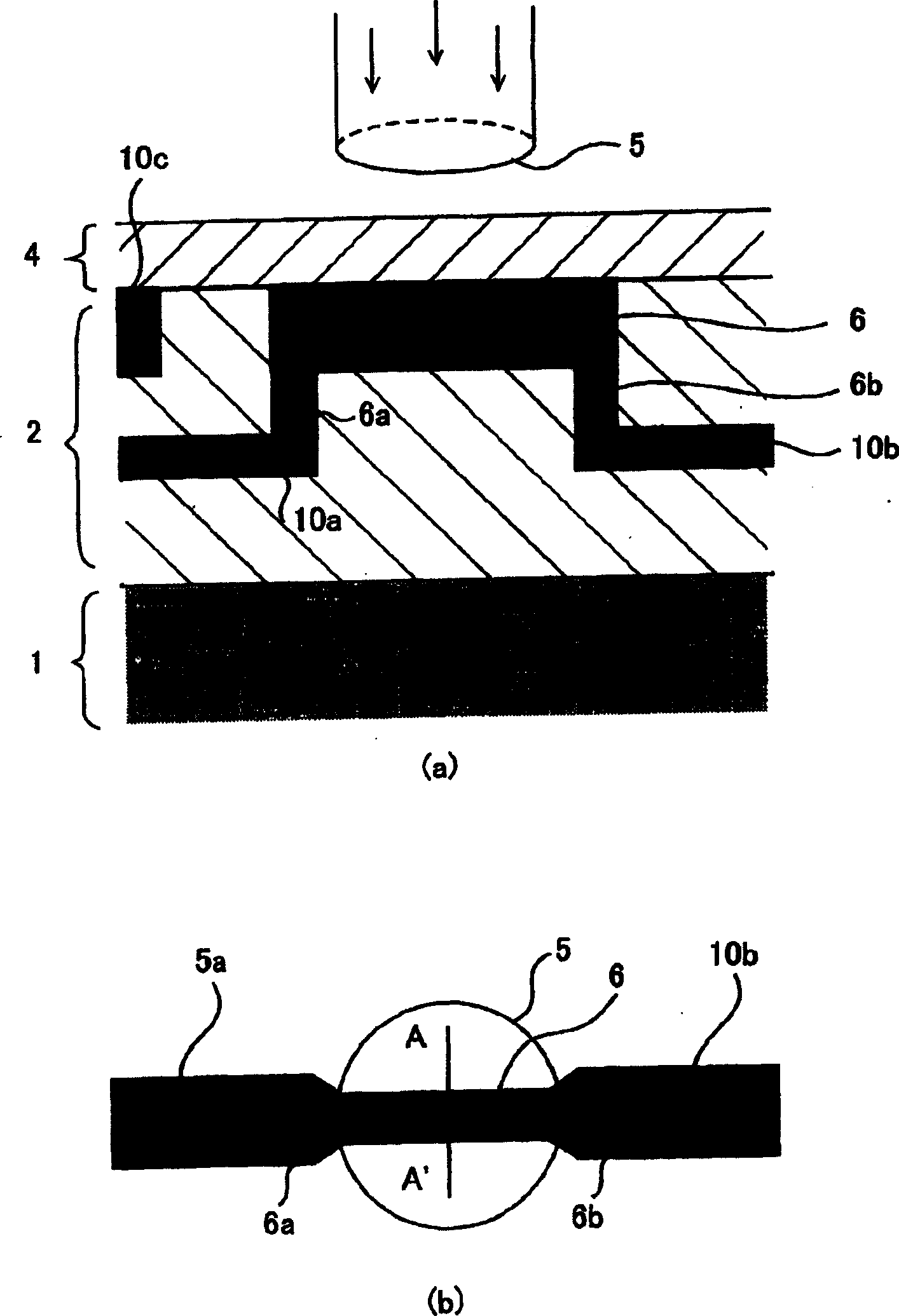
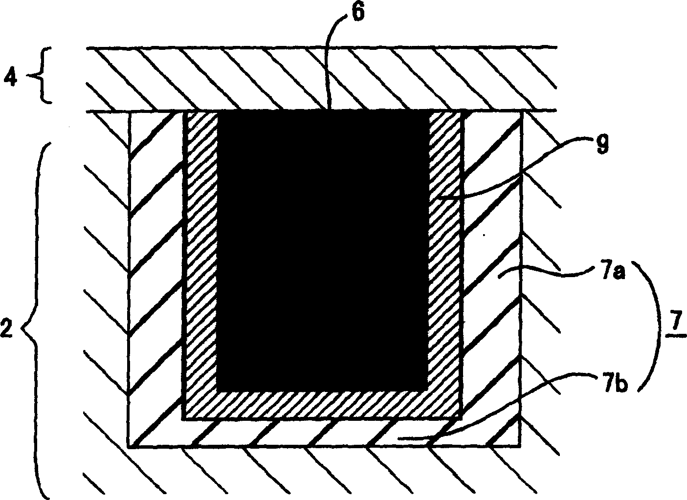
[0057] figure 1 (a) is a cross-sectional view showing a state in which the fuse related to the present invention is viewed from a lateral direction. In addition, figure 1 (b) shows the state which looked at the same area from directly above. In this figure, 2 is an interlayer insulating film (first insulating film) formed on the main surface (surface on which circuits and the like are formed) side of the silicon (semiconductor) substrate 1 . The interlayer insulating film 2 has been described as one...


PUM


Abstract

To securely burn out a fuse formed in an upper layer of a chip by laser blow using an infrared laser beam. A semiconductor integrated circuit includes a wiring member formed on a main face of a semiconductor substrate, a fusing member which is connected to the wiring member and has a prescribed thickness, a barrier member which covers the bottom face and side faces of the fusing member, a light absorbing member which covers at least side face portions of the barrier member which covers the fusing member, and an insulating member which embeds the wiring member, the fusing member, the barrier member, and the light absorbing member. The complex permittivity of the light absorbing member has a real number part that is smaller in absolute value than that of the fusing member and an imaginary number part that is larger than that of the fusing member. The thickness of the light absorbing member is preferably 50% or more and 300% or less of the thickness that shows a maximum absorption efficiency for the light used to burn out the fusing member. The light absorbing member is composed of tantalum nitride, tungsten nitride, titanium nitride, or the like.

Description

technical field [0001] The present invention relates to a semiconductor integrated circuit, and more particularly to a semiconductor integrated circuit provided with a fuse that can be blown in advance. Background technique [0002] In recent years, the integration level of semiconductor integrated circuits represented by DRAM (Dynamic Random Access Memory) or SRAM (Static Random Access Memory) has been greatly improved. Due to unpredictable defects in the manufacturing process, A drop in yield is unavoidable. As a method of avoiding this, a method of making the entire chip a good product is being put into practical use by preinstalling redundant circuits in the circuit and replacing defective memory cells in the main memory cells with spare memory cells. One of the methods is laser fusing. [0003] In laser fusing, a fuse is most commonly used as an element for converting a main memory into a backup memory. Figure 13 (a) is a view of a conventional fuse mainly composed o...

Claims


Application Information

Patent Timeline
IPC IPC(8): H01L21/82H01L23/525H01L27/10
CPCH01L23/5258H01L2924/0002H01L2924/00
Inventor 河野和史岩本猛
Owner MITSUBISHI ELECTRIC CORP
Why Eureka
Try Eureka