Sensor for detecting gas and its producing method
A technology for detecting gases and sensors, applied in the direction of material resistance, etc., can solve the problems of complex device manufacturing process, inaccurate detection, low sensitivity, etc., and achieve the effects of rapid response and recovery, simple process, and high sensitivity
- Summary
- Abstract
- Description
- Claims
- Application Information
AI Technical Summary
Problems solved by technology
Method used
Image
Examples
Embodiment 1
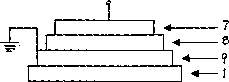
[0033] The specific structure of the sensor of the present invention can be found in figure 2 and image 3 , a polished single crystal silicon wafer is used as the substrate 1, and a layer of 0.5 μm thick diamond film / nano-diamond film 6 is grown on one side of the substrate 1; Au electrode 4, its Ti is thick 50 or 200nm, the composite metal electrode of Pt thick 100 or 400nm and Au thick 200 or 600nm; Its width is 3 or 7mm, and length is consistent with substrate width; 2 Au wire measuring leads 5 are connected in on electrode 4. A comb-shaped Pt heating resistor 2 is made on the back side of the substrate 1, and a Pt metal film with a thickness of 500-1000 nm is used to etch the metal film into Pt metal strips with a width of 10 or 50 μm. It is 15mm×15mm, and the resistance value is 0.1-5Ω; the heating resistor lead 3 made of gold is connected to the two ends of the heating resistor 2 .
Embodiment 2
[0035] The specific structure of the sensor in this embodiment can be found in figure 2 and image 3 , and in conjunction with the manufacturing method, the specific structure of the sensor of the present invention is described in detail:
[0036] (1) Make a substrate 1 on a polished single-crystal silicon wafer, vapor-deposit a 700nm metal film on its back side by sputtering, and use photolithography to etch the metal film into a Ti metal strip with a width of 25 μm. Comb-shaped heating resistor 2, two gold wires as the lead wire 3 of the heating resistor are connected to both ends of the heating resistor 2. The heating resistor 2 is designed on the one hand to make the diamond film recover as soon as possible at high temperature (300-400°C) after absorbing gas, and improve the recovery time; on the other hand, it is to improve the response time of the diamond film to gas adsorption at high temperature.
[0037] (2) After the electrode is made, make a diamond film / nano-dia...
Embodiment 3
[0041] The substrate 1 is made of a polished single-crystal silicon wafer, which also includes depositing 200-600nm silicon dioxide as an insulating layer on the substrate 1 by using a low-pressure CVD method, in order to improve measurement accuracy. All the other structures are the same as in Example 1, and the preparation method also includes the following annealing steps: placing the grown diamond film in H 2 Or annealing in H plasma: the annealing conditions are as follows: substrate temperature: 600-1000°C, H 2 Flow rate: 100-1000sccm, gas pressure: 5-60mbar, annealing time: 20 minutes-2 hours. All the other processes are the same as in Example 2. The diamond film is prepared by hot filament chemical vapor deposition (HFCVD). The diamond film containing micron / submicron crystal grains is formed on the substrate by traditional grinding or bias nucleation, using methane and hydrogen to react at high temperature. Synthetic. The nanodiamond film was prepared under DC nega...
PUM
| Property | Measurement | Unit |
|---|---|---|
| thickness | aaaaa | aaaaa |
| electrical resistance | aaaaa | aaaaa |
| width | aaaaa | aaaaa |
Abstract
Description
Claims
Application Information


