Semiconductor optical modulator and laser with optical modulator

An optical modulator, laser technology, applied in semiconductor lasers, lasers, laser parts and other directions, can solve problems such as the influence of operating temperature

Inactive Publication Date: 2004-04-21
NIPPON TELEGRAPH & TELEPHONE CORP
View PDF1 Cites 6 Cited by
  • Summary
  • Abstract
  • Description
  • Claims
  • Application Information

AI Technical Summary

Problems solved by technology

[0037] As mentioned above, conventional semiconductor light modulators are susceptible to operating temperature
Additionally, a high reverse bias voltage must be externally applied to the modulator

Method used


Image

  • Semiconductor optical modulator and laser with optical modulator
  • Semiconductor optical modulator and laser with optical modulator
  • Semiconductor optical modulator and laser with optical modulator

Examples


no. 1 example

[0064] First, a first embodiment of the present invention will be described.

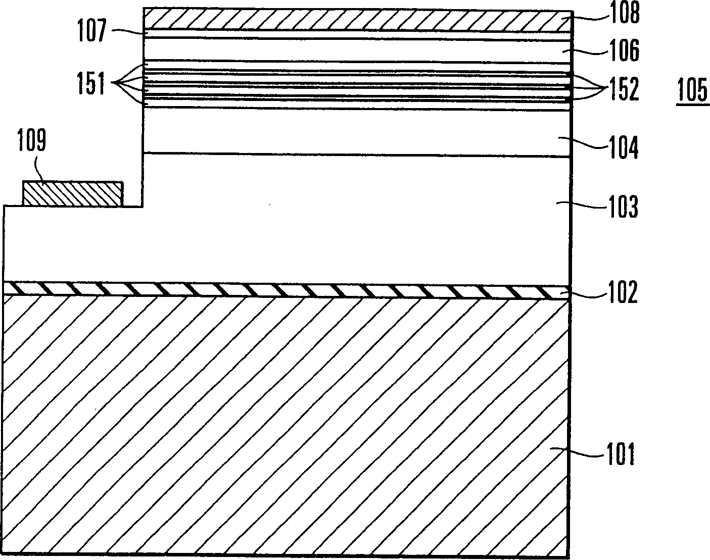
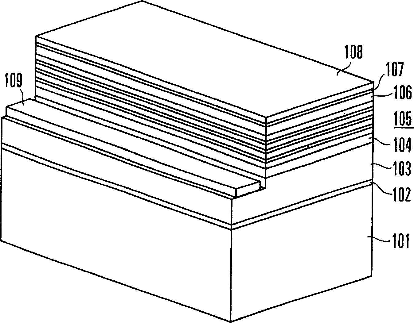
[0065] Figure 1A An embodiment according to the present invention schematically shows a structural example of a semiconductor light modulator. Figure 1B The structure of the semiconductor light modulator is schematically shown. Note that in the following description, compound semiconductor materials such as GaN, AlGaN, AlN, and InN are single crystals unless otherwise specified.

[0066] The semiconductor optical modulator is composed of (0001)-oriented sapphire (α-Al 2 o 3 crystal) with a buffer layer 102, an electrode layer 103, and a cladding layer 104 on the nitrided surface of a 330-μm-thick single crystal substrate 101. The buffer layer 102 is 20 nm thick and made of GaN. The electrode layer 103 is 4 μm thick and made of Mg-doped p-type GaN. The cladding layer 104 is 0.5 μm thick, p-type Al doped with Mg 0.1 Ga 0.9 N made. It should be noted that the single crystal substrate 101 is ...

no. 2 example

[0140] Next, another embodiment of the present invention will be described.

[0141] Figure 12 It schematically shows a structural example of a semiconductor light modulator according to another embodiment of the present invention.

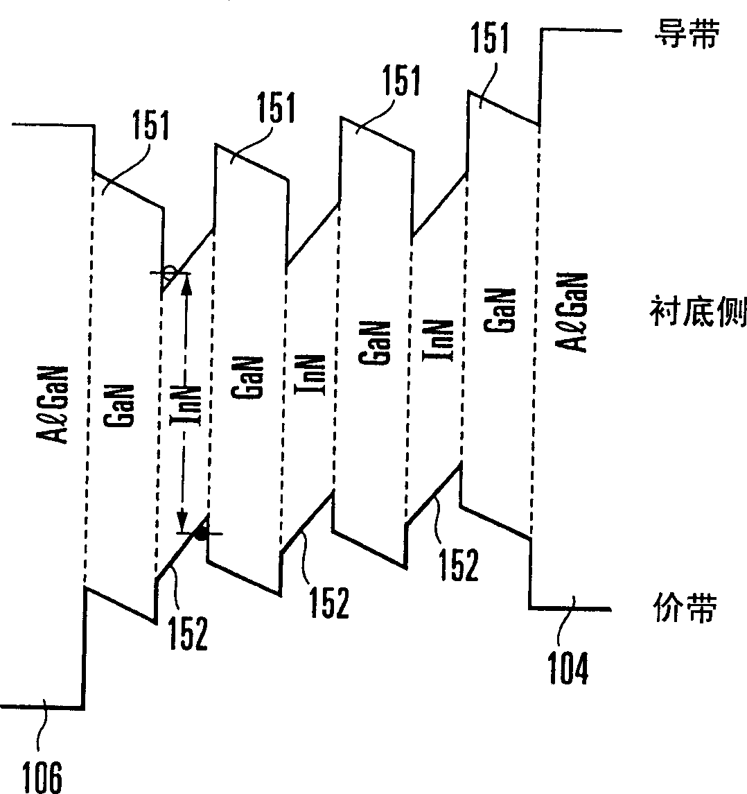
[0142] In this semiconductor light modulator, a light absorbing region in the form of a ridge is formed on the surface of a 300-μm-thick substrate 1101 made of n-type GaN. The light-absorbing region consists of the following: a lower cladding layer 1102, about 1.5 μm thick, made of Si-doped n-type Al 0.1 Ga 0.9 Made of N; 0.5-μm-thick lower SCH (Separation Suppressed Heterostructure) layer 1103 made of non-doped InGaAlN; light-absorbing layer 1104 with MQW structure; 5-μm thick made of non-doped InGaAlN The upper SCH layer 1105; p-type Al doped by Mg 0.1 Ga 0.9 a 1.5-μm-thick upper cladding layer 1106 made of N; and a 0.1-μm-thick contact layer 1107 made of Mg-doped p-type GaN. The light absorbing layer 1104 is made of In by alternating sta...


PUM

PropertyMeasurementUnit
lengthaaaaaaaaaa

Abstract

In a semiconductor optical modulator of this invention, each quantum-well layer and each barrier layer of a quantum-well structure serving as a light absorption layer are respectively made of In1-X-YGaXAlYN (0<=X, Y<=1, 0<=X+Y<=1) AND IN1-X'-Y'GaX'AlY'N (0<=X', Y'<=1, 0<=X'+Y'<=1). An electric field is being generated in the light absorption layer by spontaneous polarization.

Description

technical field [0001] The present invention relates to an optical waveguide type semiconductor optical modulator using glass fiber as a transmission medium and used for optical communication in the wavelength range of 1.3 to 1.5 μm, and a laser with the optical modulator. Background technique [0002] With the development of an advanced information society in recent years, optical communication networks using optical fibers have been developed in many countries in the world, and optical communication has performed a large amount of communication for telephone and data transmission. [0003] In order to use optical fiber to realize optical communication, a converter must be used to convert electrical signals into optical signals. The devices used for this electrical-to-optical conversion are optical modulators. [0004] Light modulation for electro-optic conversion involves modulators utilizing two schemes, direct modulation schemes and external modulation schemes. In a di...

Claims


Application Information

Patent Timeline
Patent Type & Authority Applications(China)
IPC IPC(8): G02F1/017H01S5/026
CPCG02F1/01725G02F2001/01766G02F2202/101H01S5/0265B82Y20/00G02F1/01766H01S5/34333
Inventor 松冈隆志深野秀树
Owner NIPPON TELEGRAPH & TELEPHONE CORP
Why Eureka
Try Eureka