Contact portion of semiconductor device and thin film transistor array panel for display device including the contact portion

A semiconductor and array board technology, which is applied in the field of contact parts of semiconductor devices and thin film transistor array boards for displays including the contact parts, and can solve problems such as poor contact and complicated manufacturing processes

Inactive Publication Date: 2004-04-21
SAMSUNG DISPLAY CO LTD
View PDF0 Cites 21 Cited by
  • Summary
  • Abstract
  • Description
  • Claims
  • Application Information

AI Technical Summary

Problems solved by technology

In order to solve these problems, it is preferable to make the sidewall of the contact hole in the contact portion into a stepped shape, but, for this reason, the organic insulating film must be patterned many times by the photolithography process, and the resulting problem is that the manufacturing process changes. very complicated
[0008] At the same time, it is necessary to form a seal line around the LCD panel to bond the two substrates and seal the liquid crystal material disposed therebetween. If the seal line is formed on the organic insulating film, it will cause poor contact.

Method used


Image

  • Contact portion of semiconductor device and thin film transistor array panel for display device including the contact portion
  • Contact portion of semiconductor device and thin film transistor array panel for display device including the contact portion
  • Contact portion of semiconductor device and thin film transistor array panel for display device including the contact portion

Examples


Embodiment Construction

[0047] The semiconductor device contact part of the present invention and its manufacturing method and the thin film transistor array board including the semiconductor device contact part and its manufacturing method will be described in detail according to various embodiments of the present invention below with reference to the accompanying drawings, so that those skilled in the art can easily implement.

[0048] First, a contact portion and a manufacturing method thereof will be described according to an embodiment of the present invention.

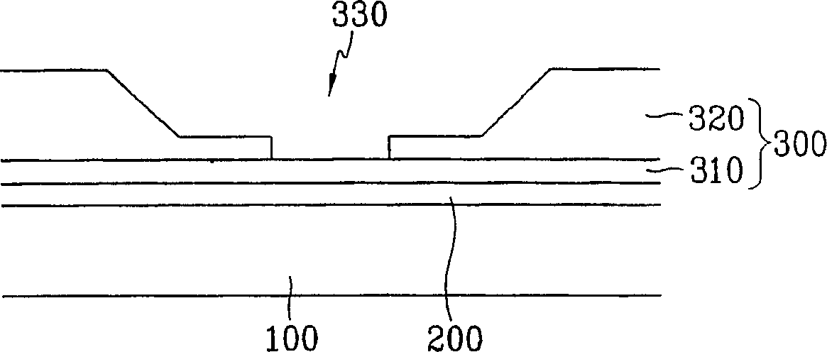
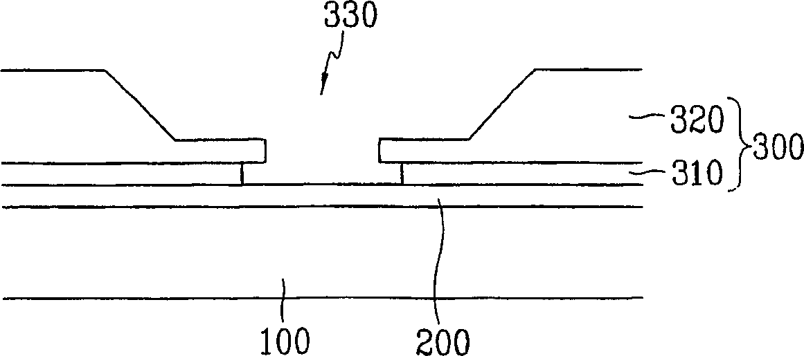
[0049] Generally, when a semiconductor device is highly integrated, it is preferable to optimize the area of ​​the device and arrange its wiring in multiple layers, so as to facilitate the connection of pads and signal lines receiving signals from external devices. A semiconductor device according to an embodiment of the present invention includes an interlayer insulating film having a low dielectric constant so as to minimize disturban...


PUM


Abstract

A gate wire is formed on a substrate. Next, after forming a gate insulating film, a semiconductor layer and an ohmic contact layer subsequently are formed thereon. Next, a data wire is formed. Next, a passivation layer and an organic insulating film are deposited, and patterned to form contact holes for exposing the drain electrode, the gate pad and the data pad, respectively. Here, the organic insulating film around the contact holes is formed thinner than that in the other portions. Next, the organic insulating film around the contact holes is removed by an ashing process to expose the borderline of the passivation layer in the contact holes, thereby removing an under-cut. Then, a pixel electrode, an assistant gate pad and an assistant data pad respectively connected to the drain electrode, the gate pad and the data pad are formed.

Description

technical field [0001] The present invention relates to a contact part of a semiconductor device and a manufacturing method thereof, and a thin film transistor array panel for a display including the contact part and a manufacturing method thereof. Background technique [0002] Generally, it is better to optimize the area of ​​the semiconductor device and arrange its wiring in multiple layers when the semiconductor device is highly integrated. In this case, it is preferable that the interlayer insulating film is made of a material having a low dielectric constant so that the interference of the signal transmitted through the wiring is minimized, and the wiring transmitting the same signal is realized through a contact hole formed in the insulating film. electrical connection. However, if an under-cut occurs on the contact portion when the contact hole is formed by etching the insulating film, the step coverage of the contact portion becomes poor. Therefore, there is a prob...

Claims


Application Information

Patent Timeline
Patent Type & Authority Applications(China)
IPC IPC(8): G02F1/1345G02F1/1362G02F1/1368H01L21/28H01L21/336H01L21/768H01L21/77H01L21/84H01L23/532H01L27/12H01L29/786
CPCH01L2924/0002H01L23/53295G02F1/13458H01L21/76802H01L21/76804G02F1/136227G02F1/136286H01L27/1214H01L27/12H01L27/1244H01L27/1248H01L2924/00H01L29/786
Inventor 金保成郑宽旭洪完植金湘甲洪雯杓
Owner SAMSUNG DISPLAY CO LTD
Why Eureka
Try Eureka