

Electrostatic discharge protecting component and method for manufacturing the same
An electrostatic discharge protection and electrostatic discharge technology, applied in semiconductor/solid-state device manufacturing, electrical components, electrical solid-state devices, etc., can solve problems such as increased cost and complex manufacturing process, reduce breakdown voltage, enhance ESD tolerance, The effect of speeding up ESD triggering
- Summary
- Abstract
- Description
- Claims
- Application Information
AI Technical Summary
Problems solved by technology
Method used
Image

Examples
no. 1 example
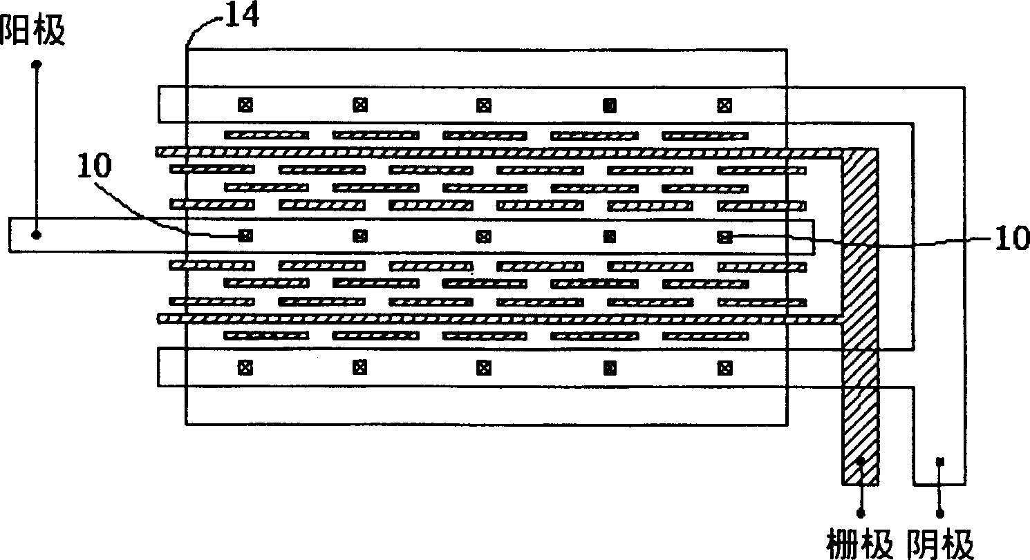
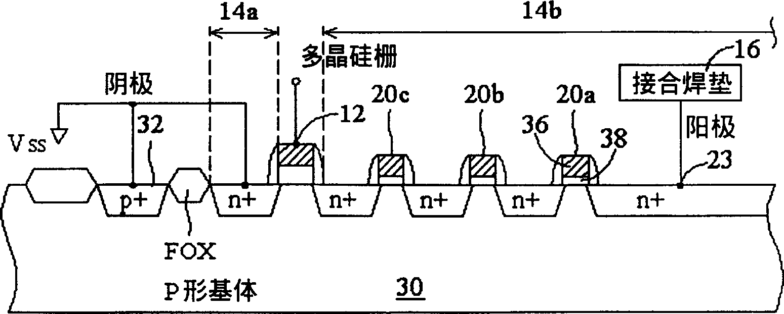
[0057] figure 2 It is an NMOS layout diagram according to the present invention. image 3 for figure 2 A schematic cross-sectional view along the line A-A'.
[0058] figure 2 The ESD protection component is a multi-finger NMOS, two polysilicon gates 12 are coupled to each other, and the gate oxide layer in the polysilicon gate 12 is a thick gate oxide layer.
[0059] The active region 14 is surrounded by an isolation region formed by a field oxide layer. The field oxide layer is mostly fabricated by local oxidation (LOCOS) or shallow trench isolation (STI) manufacturing techniques. The active region 14 is generally implanted, doped, and annealed with n-type dopants to form an n-type heavily doped (n+) layer. Ion implantation is blocked by gate structures, polysilicon blocks, or field oxides in the active region. In the active region 14 , two channel regions are formed under the two polysilicon gates 12 . The active region between the two polysilicon gates 12 is defin...
no. 2 example
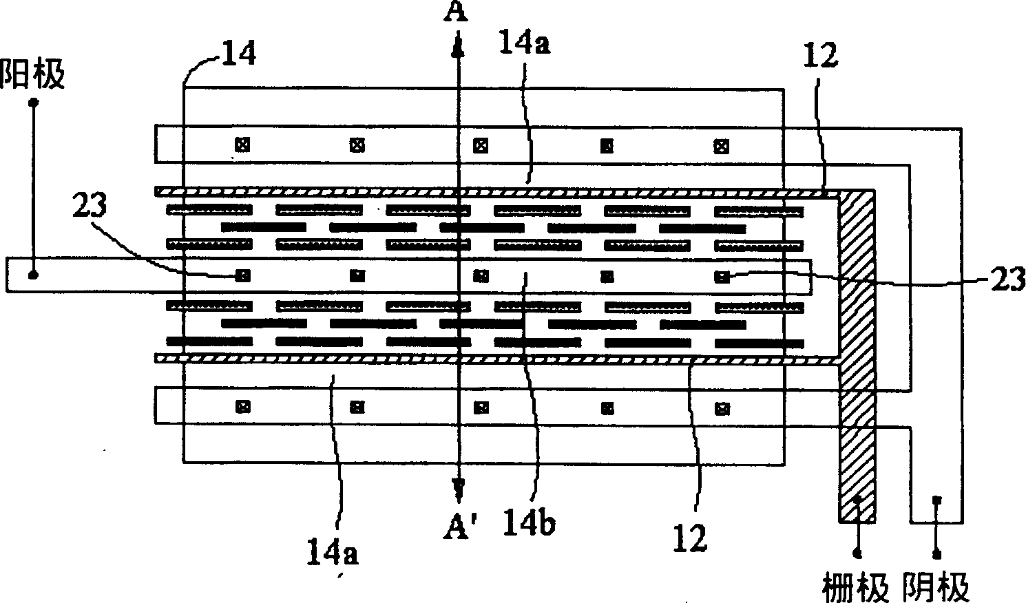
[0066] Figure 4 A layout diagram of an NMOS implemented according to the present invention is shown, wherein the oxide layer blocks in the island structure have different thicknesses. Figure 5 for Figure 4 A schematic cross-sectional view along the line A-A'.
[0067] Not all island structures need to have thin gate oxide regions. The island structure with thin oxide blocks has two main functions: 1) spread the ESD current; 2) provide a lower trigger voltage. The second function can be achieved as long as all the island structures in the drain diffusion region 14b have one island structure with a thin oxide layer section. And the first function can be achieved no matter the island structure has thick gate oxide layer block or thin oxide layer block. Therefore, in the drain diffusion region 14b, different island structures may have different thicknesses of the gate oxide layer sections. Figure 4 and Figure 5 The concept is shown in which the island structure 20a is a...
no. 3 example
[0069] Image 6 It is a layout diagram of a field device implemented according to the present invention, wherein two sides of a field gate oxide disposed above the channel area are respectively adjacent to two diffusion areas. Figure 7 for Image 6 A schematic cross-sectional view along the line A-A'.
[0070] The present invention is not limited to be applicable to NMOS generally having a control gate, but may also be applicable to NMOS of the field element type. The so-called field component means that a field oxide layer 13 is formed on the channel region, such as Image 6 as well as Figure 7 shown. Note that, Figure 7 Among them, the channel region is the base of a lateral npn bipolar junction transistor (BJT), and the diffusion regions on both sides are the collector and emitter of the npn BJT. Figure 7 and Image 6 Some of the island structures have thick gate oxide blocks and some have thin oxide blocks.
PUM
 Abstract
Description
Claims
Application Information