Method for preparing zinc oxide base magnetic semiconductor material using sub-nanometer composite method

A magnetic semiconductor, sub-nanometer technology, applied in the fields of semiconductor/solid-state device manufacturing, inorganic material magnetism, electrical components, etc., can solve the problems of material performance uncertainty, difficult control of metal ions, etc., and achieve stable performance and good repeatability. Effect

Inactive Publication Date: 2004-08-25
SHANDONG UNIV
View PDF0 Cites 9 Cited by
  • Summary
  • Abstract
  • Description
  • Claims
  • Application Information

AI Technical Summary

Problems solved by technology

The material preparation process needs to be carried out at high temperature. Due to the influence of the solid solubility of magnetic metals in ZnO, it is difficult to control the metal ions entering the ZnO lattice, resulting in the uncertainty of material properties.

Method used


Image

  • Method for preparing zinc oxide base magnetic semiconductor material using sub-nanometer composite method
  • Method for preparing zinc oxide base magnetic semiconductor material using sub-nanometer composite method
  • Method for preparing zinc oxide base magnetic semiconductor material using sub-nanometer composite method

Examples


Embodiment 1

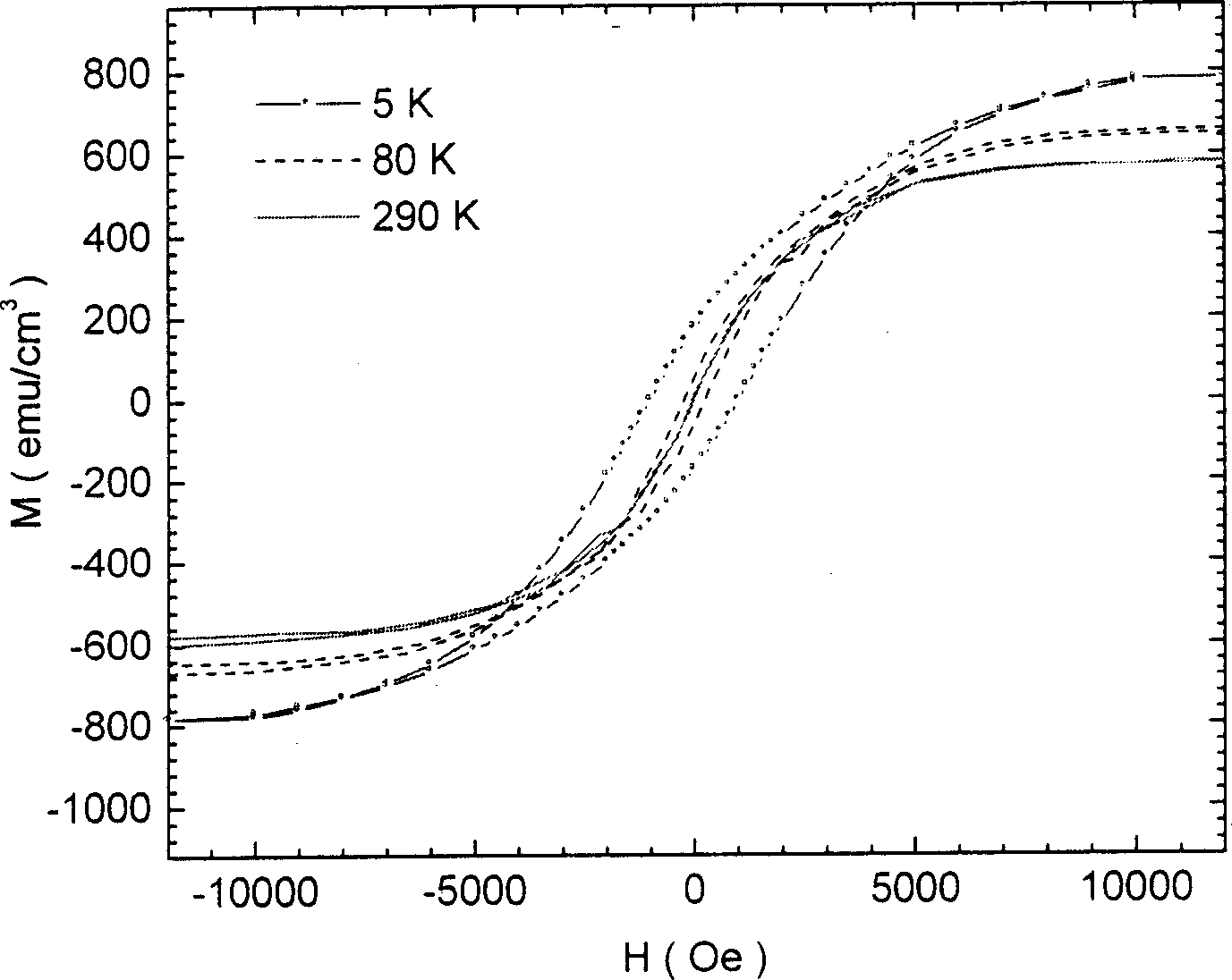
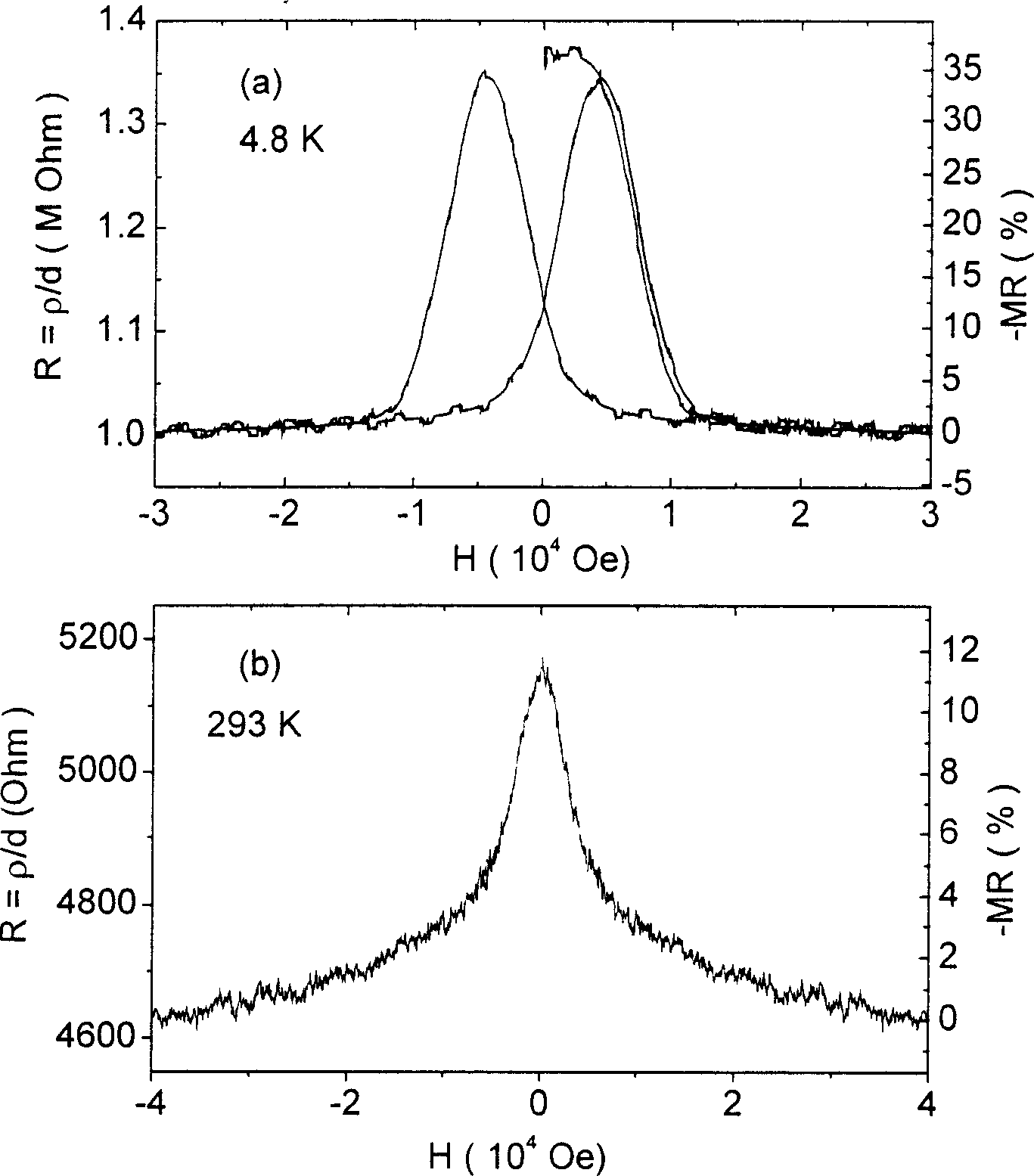
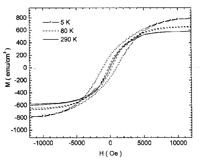
[0020] A Co-doped ZnO magnetic semiconductor (1#) was prepared by alternately growing Co and ZnO thin films on a room temperature quartz glass substrate by magnetron sputtering. The Co layer was prepared by DC sputtering with a growth rate of 0.05nm / s. The thickness is 0.6nm; ZnO is prepared by radio frequency sputtering, the growth rate is 0.02nm / s, and the thickness is 0.5nm. Grow for 60 cycles.

Embodiment 2

[0022] Using molecular beam epitaxy and laser molecular beam epitaxy to alternately grow Fe and ZnO thin films on room temperature single crystal silicon substrates, a Fe-doped ZnO magnetic semiconductor (2#) was prepared. The Fe layer was prepared by molecular beam epitaxy, and the growth rate was 0.01nm / s, thickness 0.1nm; ZnO is prepared by laser molecular beam epitaxy, growth rate is 0.005nm / s, thickness 0.3nm. Grow for 120 cycles.

Embodiment 3

[0024] The FeNi-doped ZnO magnetic semiconductor (3#) was prepared by alternately growing FeNi and ZnO thin films on a common glass substrate at room temperature by magnetron sputtering. The FeNi layer was prepared by DC sputtering with a growth rate of 0.04nm / s and a thickness of 0.2nm; ZnO is prepared by radio frequency sputtering with a growth rate of 0.02nm / s and a thickness of 0.8nm. 80 cycles of growth.


PUM

PropertyMeasurementUnit
thicknessaaaaaaaaaa
thicknessaaaaaaaaaa
thicknessaaaaaaaaaa

Abstract

This invention relates to a sub-nm compound method for preparing ZnO base magnetic semiconductor film materials by magnetic control sputtering, molecular beam epitaxial, laser pulse deposition or laser molecular beam epitaxial method to alternately deposit the sub-nm transition metal and ZnO high-gap semiconductor layer on the substrate and compound then at atom size to form a magnetic semiconductor, the transition metal is from Co, Fe, Ni or Mn or their alloy. Compared with other methods, this invented material is grown under low temperature and non-balanced condition, the dope to the transition metal is not limited by solid solubility.

Description

(1) Technical field [0001] The invention relates to a method for preparing a ZnO-based semiconductor film material by using a sub-nanometer composite method, and belongs to the technical field of electronic materials. (2) Background technology [0002] Traditional microelectronics is based on the charge characteristics of electrons, and the spin information of electrons is not considered. Since the 1990s, the spin transport properties of electrons have attracted the attention of researchers, and people began to consider using the spin properties of electrons to develop new electronic devices. Since the semiconductor-based microelectronics technology is very mature, it is of great significance to prepare spintronic devices with new functions using traditional semiconductor processes and materials. Research in this area mainly focuses on two directions: one is to prepare carrier spin-polarized semiconductor materials, that is, magnetic semiconductors; the other is to combine ...

Claims


Application Information

Patent Timeline
Patent Type & Authority Applications(China)
IPC IPC(8): H01F1/40H01L21/203
Inventor 梅良模颜世申陈延学任妙娟季刚
Owner SHANDONG UNIV
Why Eureka
Try Eureka