Metal mask plate

A metal mask, metal mask technology, applied in optics, instruments, opto-mechanical equipment, etc., can solve the problems of troublesome and complicated production, high cost, expensive investment, etc., so as to reduce the cost of lithography equipment and reduce the difficulty of production technology Effect

Inactive Publication Date: 2004-12-08
INST OF OPTICS & ELECTRONICS - CHINESE ACAD OF SCI
View PDF0 Cites 18 Cited by
  • Summary
  • Abstract
  • Description
  • Claims
  • Application Information

AI Technical Summary

Problems solved by technology

However, these methods require extremely short-wavelength light source electromagnetic radiation systems and optical systems, which are not only very complicated in technology, but also very expensive in investment. Troublesome and complicated, it requires proximity effect correction technology, and resolution enhancement technology such as phase shift

Method used


Image

  • Metal mask plate
  • Metal mask plate
  • Metal mask plate

Examples


Embodiment Construction

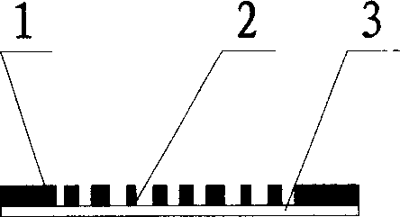
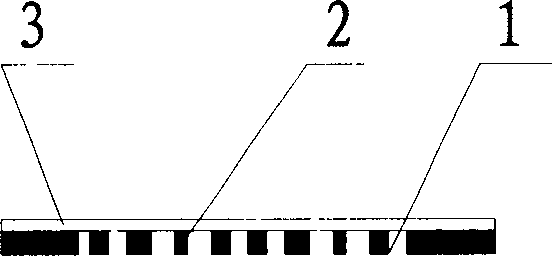
[0018] Such as figure 1 As shown, embodiment 1 of the present invention is made up of chromium mask pattern thin layer 2, the sio2 film or substrate 3 positioned below and the metal mask pattern book layer 1 with the same pattern as the chromium mask pattern layer 2 above, wherein The thickness of the sio2 thin film or substrate 3 is at least 1 μm, the thickness of the chromium mask pattern thin layer 2 is 5-150 nm, and the metal material of the metal mask pattern book layer 1 is gold, silver or copper or aluminum, and its thickness is 5 nm. -150nm. The general wavelength or long wavelength laser can pass through the nanometer metal mask whose pattern size is much smaller than the wavelength, because the metal mask with ultrafine pattern produces a surface with a very short wavelength under the irradiation of general wavelength or long wavelength laser. Plasma wave, the plasma wave can pass through the holes and slots of the thin layer 2 pattern of the nano-chromium mask patt...


PUM

PropertyMeasurementUnit
Thicknessaaaaaaaaaa
Thicknessaaaaaaaaaa

Abstract

A mask plate comprises base plate, top surface or bottom surface and metal film layer pattern of chromium and gold or copper or silver or aluminium in the same pattern at both of top and bottom surfaces. It works as that a light is used to shine metal mask plate with micro-fine pattern structure to generate plasma wave in short wavelength for carrying out photoetching with normal wavelength light or long wavelength light passing through metal mask based on propagation characteristic of nanopattern hole and seam.

Description

technical field [0001] The invention relates to a metal mask plate for producing ultrafine patterns by a photolithographic exposure system and an application thereof, and belongs to the technical field of masks for producing ultrafine patterns by microfabrication technology. Background technique [0002] With the rapid development of global communication technology and high-tech information technology, there is an urgent need for microfabrication technology to produce ultra-high-speed, ultra-high-frequency nanoscale IC devices. Fabrication of nano-IC devices requires a substantial increase in the resolution of existing lithography techniques. Due to the limitation of the diffraction limit, when the hole size of the mask pattern is much smaller than the wavelength of the nanopattern, the light cannot pass through the hole, so the nanopattern photolithography cannot be performed. Therefore, the method of shortening the wavelength lithography is generally used to improve the r...

Claims


Application Information

Patent Timeline
IPC IPC(8): G03F1/62G03F7/00G03F7/20
Inventor 陈旭南罗先刚秦涛陈元培杜春雷
Owner INST OF OPTICS & ELECTRONICS - CHINESE ACAD OF SCI
Why Eureka
Try Eureka