
ZnO based transparent thin film transistor and its prepn. method

A thin-film transistor and thin-film technology, which is applied in the field of ZnO-based thin-film transistors and their preparation, can solve problems such as restricted fields of work, opacity, etc., and achieve the effects of cost reduction, simple production process, and easy application.

Inactive Publication Date: 2005-01-12
ZHEJIANG UNIV
View PDF0 Cites 11 Cited by
  • Summary
  • Abstract
  • Description
  • Claims
  • Application Information

AI Technical Summary

Problems solved by technology

However, due to its opacity, Si material is easily affected by visible light photoinduced leakage current, which limits its working field.

Method used


Image

  • ZnO based transparent thin film transistor and its prepn. method

Examples


Embodiment Construction

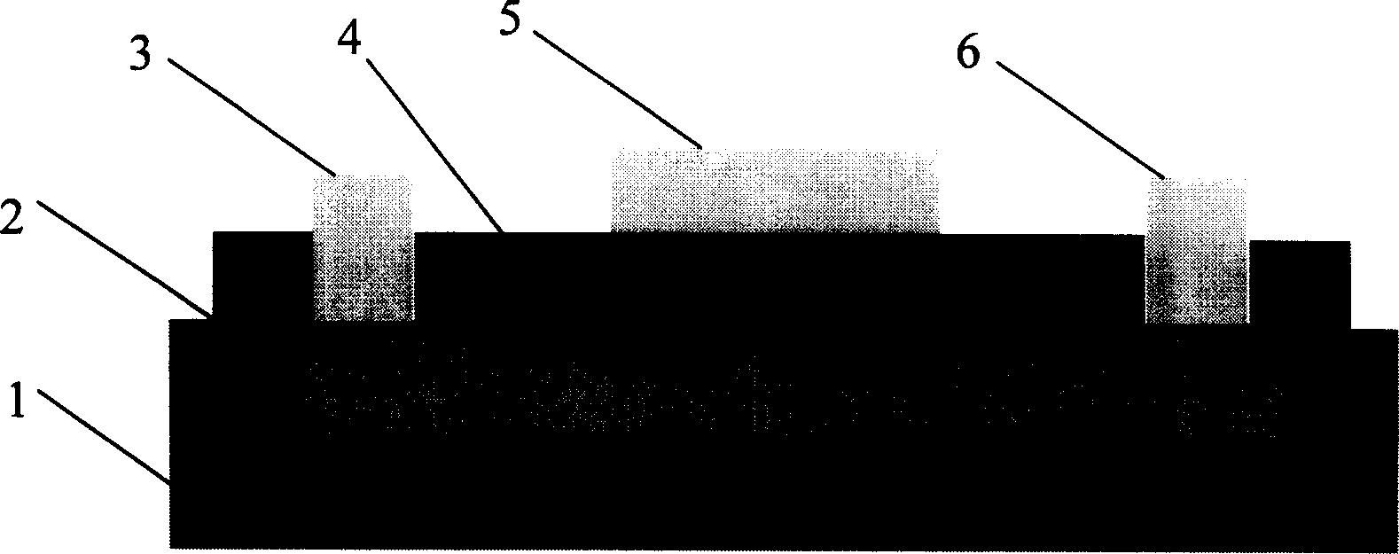
[0016] Refer to attached figure 1 , illustrating the structure and implementation method of the ZnO-based thin film transistor of the present invention: deposit n-ZnO thin film 2 on the substrate 1, and then conduct the first photolithography to separate small transistor units. Then rapid thermal annealing (RTA) (600-800°C O 2 atmosphere) to increase the channel resistance and improve the crystallization properties of ZnO. Then uniformly coat a layer of photoresist on the surface, engrave a pattern with a photolithography layout, and then deposit a layer of ATO film 4 as a gate insulating layer, and engrave an electrode window by a lift-off process. Then rapid thermal annealing (RTA) (600-800°C O 2 atmosphere) to improve the electrical properties of the ATO / ZnO interface. Then deposit the ITO thin film transparent electrode, and use wet photolithography to form the source electrode 3, the gate electrode 5, and the drain electrode 6. Rapid thermal annealing at 300°C is then...


PUM

PropertyMeasurementUnit
Thicknessaaaaaaaaaa

Abstract

n-ZnO film in 50-150nm thickness deposited on glass substrate is as channel of thin film transistor (TFT). ATO film is as gate insulation layer, and ITO film is adopted in source, gate and drain poles. light transmittance in the transparent TFT reaches to more than 80% in visible light region. Comparing with general Si TFT, the invention prevents photo-electron leakage current generated between source and drain poles caused by incident light so that cutting off current will not rise. Features are: simple technique, suitable to active matrix LCD.

Description

technical field [0001] The invention relates to a ZnO-based thin film transistor transparent in the visible light region and a preparation method thereof. Background technique [0002] In recent years, the research on ZnO, a compound semiconductor with a wide bandgap, has been extremely active. Since ZnO has a high exciton binding energy (60 mev at room temperature), the exciton gain can also reach 300cm -1 , is an ideal short-wavelength light-emitting device material, and has great application potential in the fields of light-emitting diodes (Light-emitting Diodes), laser LDs (Laser Diodes) and other fields. On the other hand, many intrinsic donor defects (such as zinc interstitials and oxygen vacancies) of ZnO will produce high self-compensation, so it is very difficult to achieve stable p-type doping, which restricts its rapid industrialization in light-emitting devices. Traditional thin-film transistors usually use amorphous silicon (α-Si TFT), which is the most researc...

Claims


Application Information

Patent Timeline
IPC IPC(8): H01L21/336H01L29/786
Inventor 叶志镇袁国栋朱丽萍钱庆
Owner ZHEJIANG UNIV
Learn More