Method of making liquid crystal display

A technology of liquid crystal display and manufacturing method, which is applied to static indicators, instruments, transistors, etc., can solve the problems of difficulty in controlling the leakage current, complicated manufacturing process, and low image quality, so as to avoid risks and probability, improve Electrical performance, the effect of simplifying the process

Inactive Publication Date: 2005-01-19
TPO DISPLAY
View PDF0 Cites 19 Cited by
  • Summary
  • Abstract
  • Description
  • Claims
  • Application Information

AI Technical Summary

Problems solved by technology

So many manufacturing steps make the manufacturing process very complicated. At the same time, each time the photoresist layer is formed, a yellowing process is required, and each yellowing process actually has the risk of misalignment. , after such a complex and multiple yellowing process, it is difficult for the components produced to be free of defects
In particular, the lightly doped drain part is often asymmetrical in width due to the alignment error in manufacturing the gate electrode and the alignment error in manufacturing the source electrode and drain electrode of the thin film transistor in the pixel array region. (asymmetry) situation, causing components to be broken down early
In addition, although the manufacturing method of integrating complementary metal oxide semiconductor transistors in the prior art is a common manufacturing method following the integrated circuit industry, it includes both N-type metal oxide semiconductor transistors and P-type metal oxide semiconductor transistors. In the circuit manufacturing method of the material semiconductor transistor, it is really impossible to significantly reduce the number of the yellow light process and the ion implantation process, and at the same time, the leakage current (leakage current) of the N-type low-temperature polysilicon thin film transistor itself is not easy to be controlled, so it is applied in In the pixel area, the image quality is often not high

Method used


Image

  • Method of making liquid crystal display
  • Method of making liquid crystal display
  • Method of making liquid crystal display

Examples


Embodiment Construction

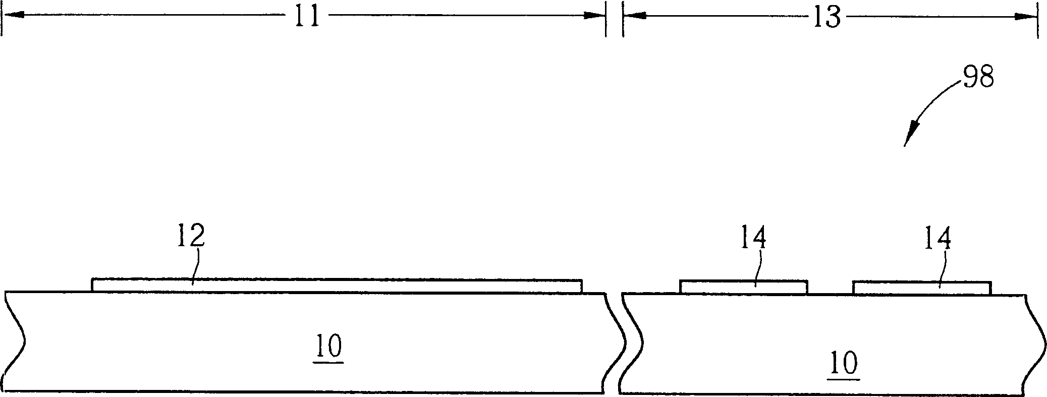
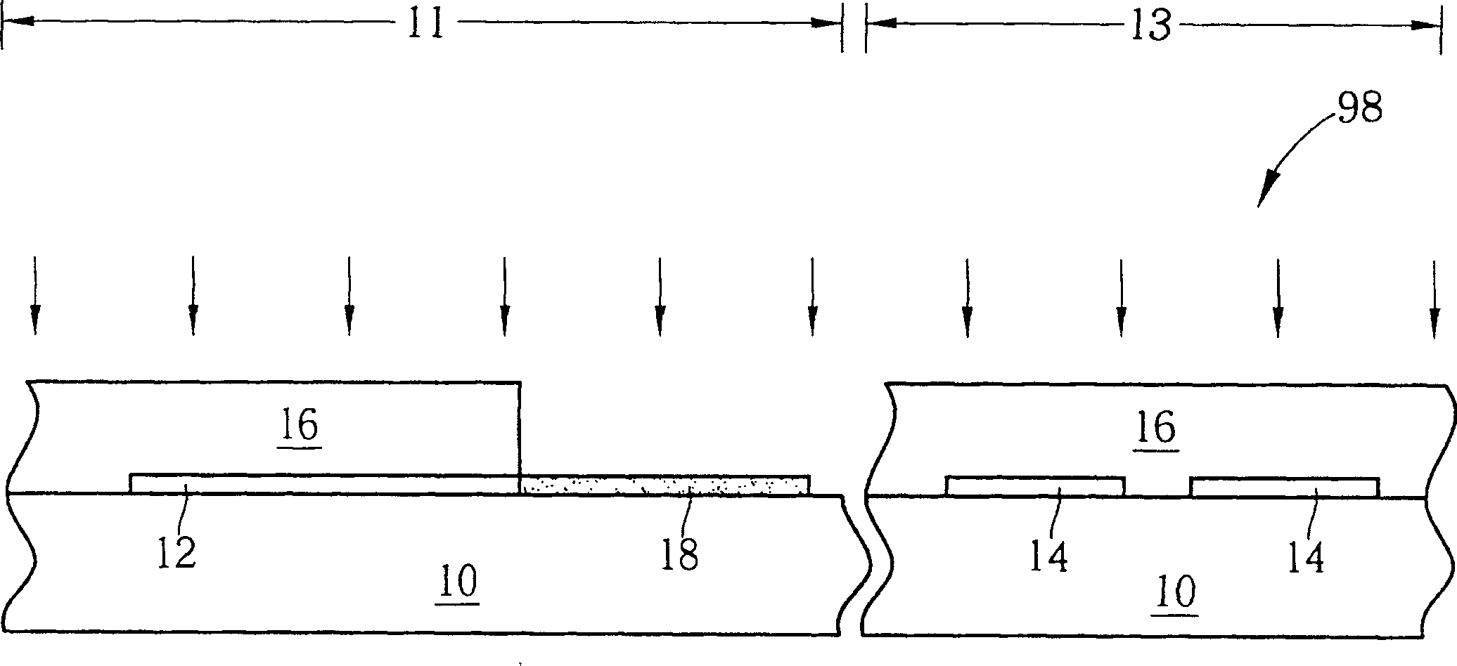
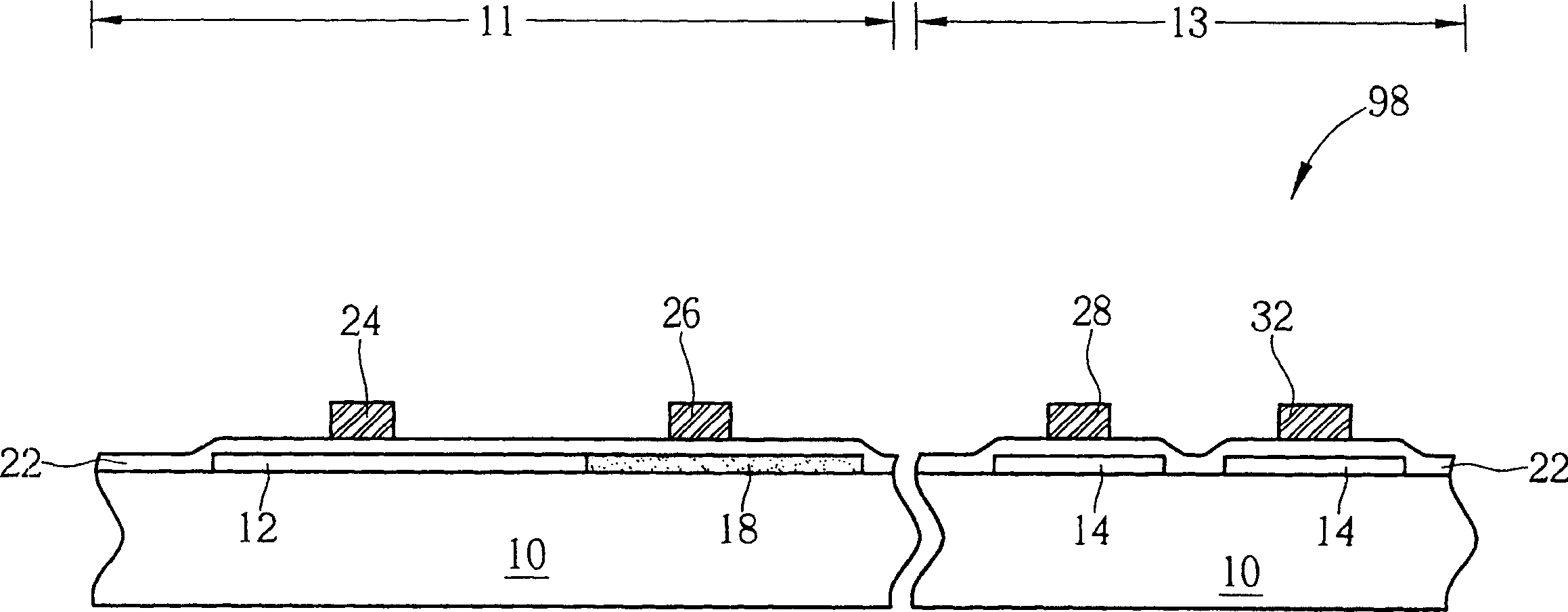
[0064] Please refer to Figure 9 to Figure 13 , Figure 9 to Figure 13 It is a schematic diagram of a method of manufacturing a low-temperature polysilicon thin film transistor liquid crystal display 174 in the first embodiment of the present invention. Such as Figure 9 As shown, the low-temperature polysilicon thin film transistor liquid crystal display of the present invention is manufactured on an insulating substrate 100. The insulating substrate 100 must be made of a light-transmitting material, usually a glass substrate or a quartz substrate, and the surface of the insulating substrate 100 includes a pixel. The array area 101 and a peripheral circuit area 103 .

[0065] In the present invention, an amorphous silicon film (not shown) is first formed on the surface of the insulating substrate 100 by a sputtering process or other processes, and then an excimer laser annealing process is performed to recrystallize the amorphous silicon film (not shown). into a polysilico...


PUM


Abstract

This invention relates to a process method of LCD, which are the following: first to form the source layer of a P-shaped low-temperature poly-silicon film transistor and down memory electrode; then to separately form P-shaped source and drain electrodes and inject adulterant into down memory electrode; later to form grating insulation layer, grating electrode, capacity dielectric layer and upper memory electrode; finally to form source electrode wire of the LCD, leak electrode wire and pixel electrode .

Description

technical field [0001] The present invention relates to a method for manufacturing a low temperature polysilicon thin film transistor liquid crystal display (LTPS TFT-LCD), in particular to a method for manufacturing a low temperature polysilicon thin film transistor liquid crystal display (LTPS TFT-LCD) using seven yellow light processes and consisting entirely of P-type low temperature polysilicon thin film transistors A method of manufacturing a liquid crystal display. Background technique [0002] Among today's flat panel display technologies, liquid crystal display (LCD) can be said to be the most mature technology. For example, mobile phones, digital cameras, video cameras, notebook computers and even monitors that are common in daily life are Products manufactured using this technology. However, with the improvement of people's requirements for display visual experience and the continuous expansion of new technology application fields, flat-panel displays with higher...

Claims


Application Information

Patent Timeline
Patent Type & Authority Applications(China)
IPC IPC(8): G02F1/133G02F1/136H01L29/786
Inventor 石储荣林国隆陆一民
Owner TPO DISPLAY
Why Eureka
Try Eureka