Method of manufacturing bus electrode of plasma display board

A bus electrode and plasma technology, which is applied in the production field of plasma display panel bus electrodes, can solve the problems of complex thin-film photolithography process, low material utilization rate, and long production cycle, and achieve small space occupation and high material utilization rate. The effect of high and huge equipment

Inactive Publication Date: 2005-03-23
SOUTHEAST UNIV
View PDF0 Cites 5 Cited by
  • Summary
  • Abstract
  • Description
  • Claims
  • Application Information

AI Technical Summary

Problems solved by technology

The above three fabrication methods of bus electrodes have disadvantages: Both the screen printing method and the photosensitive silver paste method need to go through a high-temperature sintering process at about 450°C to remove the organic solvent and adhesive in the conductive silver paste, and to make the paste in the paste The low melting point glass is fused with silver powder, so that the silver can be firmly attached to the substrate
High temperature sintering process has long production cycle and high cost
Compared with the screen printing method, the photosensitive silver paste method has higher precision, but the material utilization rate is low and the waste is large
The thin film photolithography process is more complicated, the production cycle is long, and the investment cost is high

Method used


Image

  • Method of manufacturing bus electrode of plasma display board
  • Method of manufacturing bus electrode of plasma display board
  • Method of manufacturing bus electrode of plasma display board

Examples


specific Embodiment approach

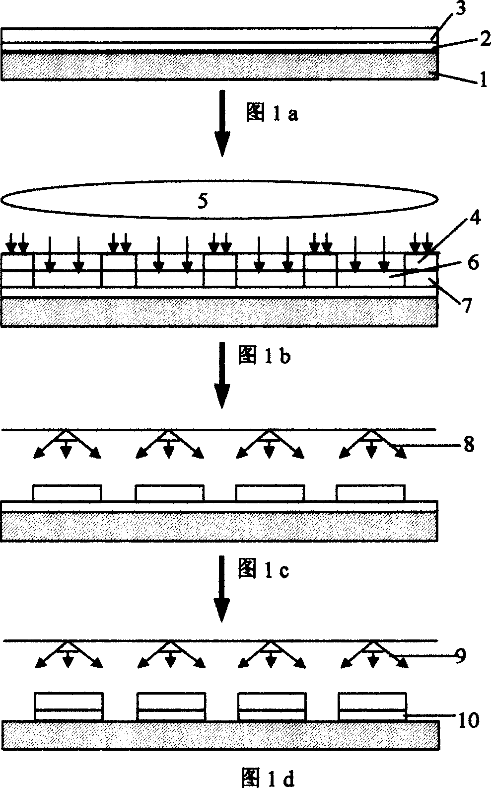
[0025] The substrate is cleaned, and the substrate includes a base glass substrate 1 and a transparent conductive film 2 covered on its surface.

[0026] The photosensitive adhesive 3 is hot-pressed on the surface of the transparent conductive film 2, and the adhesive film should be smooth without air bubbles.

[0027] Exposure: spread the mask plate 4 with line graphics on the surface of the photosensitive adhesive 3 and press it tightly so that the photosensitive adhesive 3 and the mask plate 4 have no gap. Then use ultraviolet light 5 to irradiate mask plate 4 and photosensitive adhesive 3 vertically, ultraviolet light 5 can penetrate the transparent area on mask plate 4 and irradiate the corresponding parts of photosensitive adhesive 3, so that this part of photosensitive adhesive is cured to form a cured The photosensitive glue 6 ; the opaque area on the mask plate 4 can block the irradiation of the ultraviolet light 5 and keep the corresponding parts of the photosensitiv...


PUM

PropertyMeasurementUnit
Thicknessaaaaaaaaaa

Abstract

The production method of the Plasma Display Panel junction electrode is the production method of the alternating and direct current Plasma Display Panel accordant junction electrode during producing the alternating and direct current Plasma Display Panel. Its production method includes the following steps: a. spread the sensitization glue on the transparent conductive film covered on the surface of the basal lamina; b. exposure: spread the masking board with line drawing on the surface of the sensitization glue and irradiate the masking board and sensitization glue with ultraviolet light; c. developing: spray the processed basal lamina with the photographic developer and get rid of the petrified sensitization glue; d. etching: spray the developed basal lamina with etching solution; e. plating: plate the junction electrode on both sides of the transparent current-carrying electrode; f. stripping of photoresist: put the plated things into the stripping of photoresist solution, marinate it for several minutes, get rid of the petrified sensitization glue on the surface of the transparent current-carrying electrode and finish preparing the junction electrode.

Description

technical field [0001] The present invention relates to a method for manufacturing bus electrodes of AC and DC plasma display panels during the manufacturing process of AC and DC plasma display panels, and belongs to the field of plasma display panel manufacturing. [0002] technology field. Background technique [0003] In order to reduce the resistance of the transparent conductive electrode on the front substrate of the plasma display panel, a layer of bus electrode is usually made on the transparent conductive electrode, and a metal material with good conductivity is generally used. The conventional methods include screen printing method, photosensitive silver paste method and thin film photolithography. The screen printing method makes the required electrode pattern on a certain mesh screen by means of exposure and development, uses the conductive silver paste as the raw material of the bus electrode, and then prints the conductive silver paste on...

Claims


Application Information

Patent Timeline
IPC IPC(8): H01J9/02
Inventor 樊兆雯张雄李青王保平
Owner SOUTHEAST UNIV
Why Eureka
Try Eureka