

Ridge waveguide semiconductor optical device and manufacuring method
A ridge waveguide and semiconductor technology, which is applied in the direction of semiconductor devices, optical waveguide semiconductor structures, electrical components, etc., can solve the problems of difficult completion, high technical requirements, high cost, etc., and achieve simplified preparation process steps and low process technical requirements. High, the effect of improving contact performance
- Summary
- Abstract
- Description
- Claims
- Application Information
AI Technical Summary
Problems solved by technology
Method used
Image

Examples
Embodiment Construction
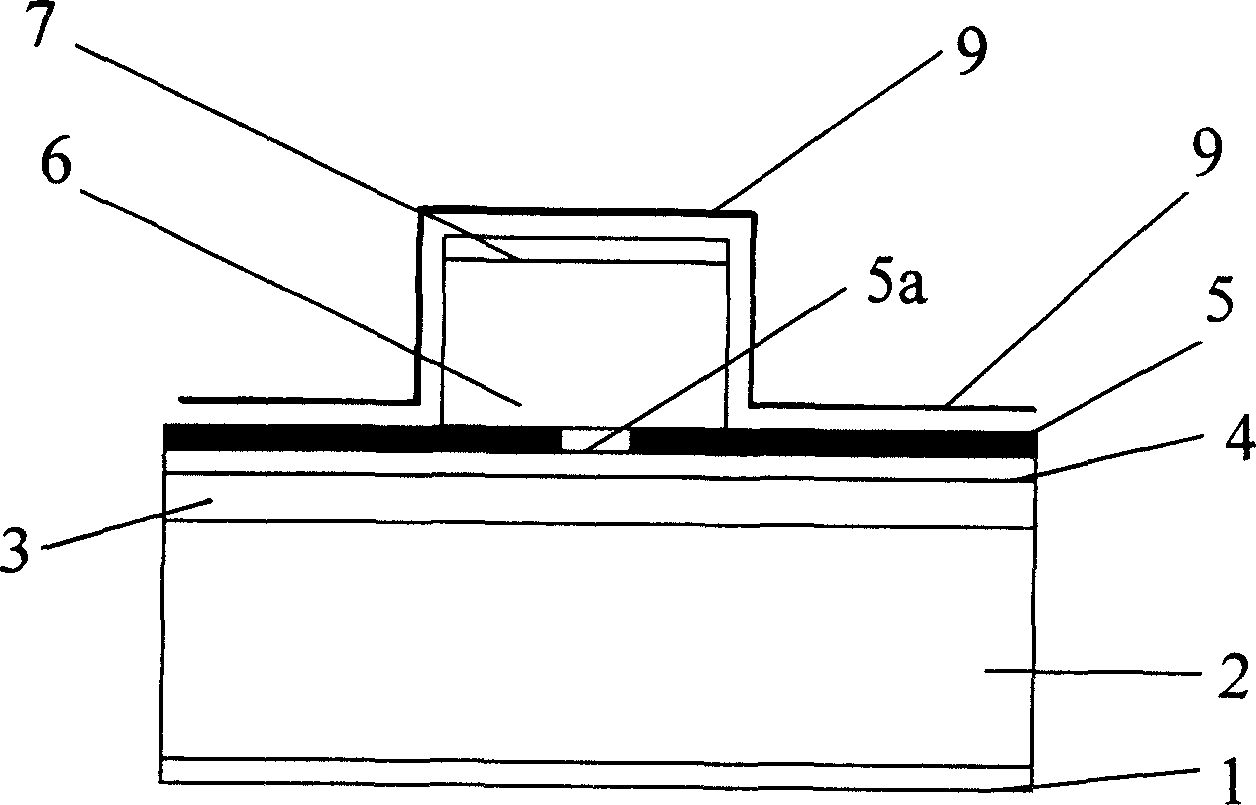
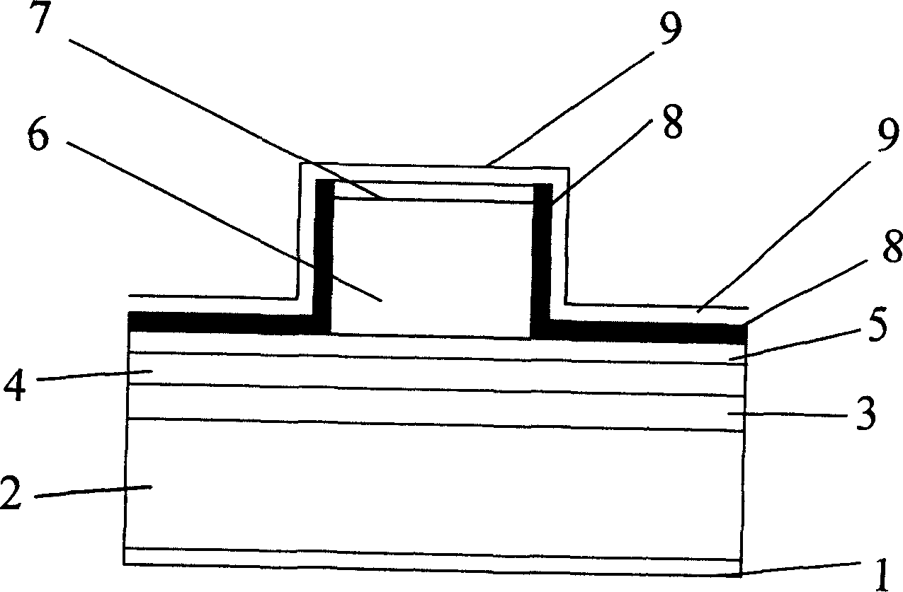
[0028] see figure 1 , the semiconductor laser in this embodiment has a layered structure, the same as the prior art, the layered structure is also followed by the lower electrode layer 1, the semiconductor substrate layer 2, the active layer 3 and the upper coating layer from bottom to top. Layer 4. Among them, the function of the active layer 3 is mainly to provide light gain, and the function of the upper coating thin layer 4 and the upper coating thick layer 6 is to limit light waves.
[0029] figure 1 It is shown that in this embodiment, the difference from the prior art is that there is a planar insulating layer 5 above the upper coating thin layer 4, and a current injection channel 5a with adjustable width is provided in the center of the planar insulating layer 5. Above the insulating layer 5, with the current injection channel 5a as the center, there is a ridge-shaped upper coating thick layer 6, and the upper coating thick layer 6 is the current contact layer 7, a...
PUM
 Abstract
Description
Claims
Application Information