
Photovoltaic cell interconnection

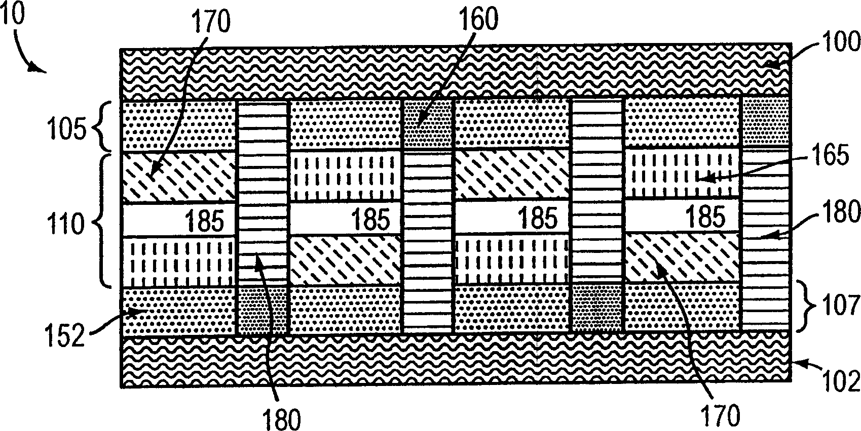
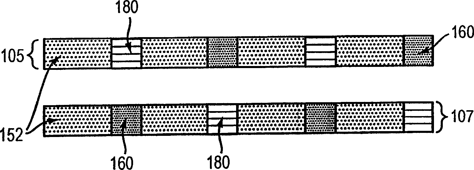
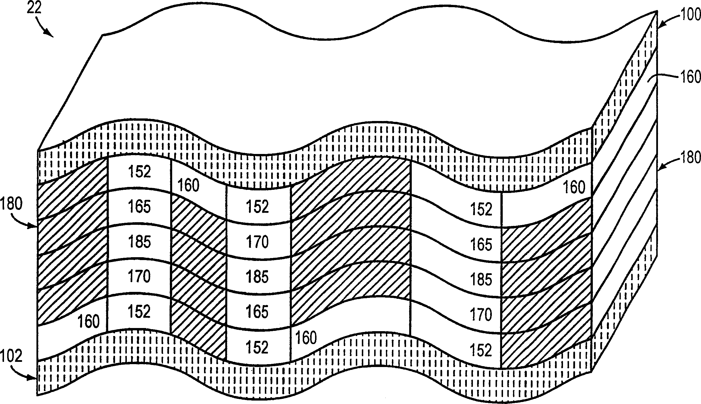
A technology of photovoltaic cells and electrical connection layers, applied in photovoltaic power generation, primary batteries, circuits, etc., can solve the problems of upper boundary limit of photovoltaic module performance, increase of manufacturing failure, reduction of energy capture area, etc.

Inactive Publication Date: 2005-07-20
KONARKA TECHNOLOGIES
View PDF0 Cites 7 Cited by
  • Summary
  • Abstract
  • Description
  • Claims
  • Application Information

AI Technical Summary

Problems solved by technology

Currently used techniques require laser or mechanical scribing to cut some areas of the preformed photovoltaic cell, which increases the risk of manufacturing failure and increases the cost
Further, using cutting or selectively depositing and removing material often results in waste of useful material
As a result, the energy trapping area in optoelectronic devices is reduced, and the upper bound of optoelectronic module performance is limited

Method used


Image

  • Photovoltaic cell interconnection
  • Photovoltaic cell interconnection
  • Photovoltaic cell interconnection

Examples


Embodiment 1

[0078] Dye-sensitive solar cells have flexible substrates made according to the following procedure.

[0079] The thickness of the PET substrate is about 200 microns, about 10 mm x 10 mm square covered with about 200 nm thick ITO coating by thermal evaporation. By diffusing P25 (a commercially available crystalline TiO containing about 80% anatase and 20% rutile) in water (pH 3-4) 2 Titanium dioxide) to produce colloidal TiO 2 solution. TiO 2 Nanoparticle layers were formed on PET substrates by spin-coating deposition. To prepare the dispersion of the nanoparticles, it is possible to use, for example, microfluidization techniques, attrition techniques or ball milling techniques. After deposition the coating is heated to about 50°C for about 1 minute or less.

[0080] Coated with TiO 2 The PET substrate was then covered with a crosslinker solution containing 0.3 mM tetrabutyltitanium oxide solution in alcohol to attach the nanoparticles. The coated substrate was dried at...

Embodiment 2

[0083] Dye photosensitive photovoltaic cells with rigid substrates were fabricated according to the following steps.

[0084] Glass plate coated with ITO coating (surface resistance 8Ω / cm 2 ) by a layer through from TiO 2 Dispersion spin-coated about 10 µm thick TiO 2 (P25) Nanoparticle film covering. The coated slides were allowed to dry at room temperature for approximately 30 minutes and sintered in an oven at approximately 450°C for 1 hour for bonding.

[0085] The sintered slides were passed through a solution of cis-bis(thiocyanate)bis(2,2′-dipyridyl-4,4′-dicarboxylate)ruthenium(II) in alcohol (1 mg / mL) Soak slides in medium overnight to render dye photosensitizing.

[0086]A redox polyelectrolyte (10% polyethylene oxide, 90% 1:1 ethylcarbonate:propylcarbonate, 0.05M iodine and 0.5M LiI) was coated on the substrate, sandwiched between coated with A second glass plate with an ITO conductive layer about 200 nm thick and a platinum catalytic layer about 2.5 nm thick. ...


PUM

PropertyMeasurementUnit
sizeaaaaaaaaaa
sizeaaaaaaaaaa
glass transition temperatureaaaaaaaaaa

Abstract

The invention, in one aspect, provides a photovoltaic cell including a charge carrier material and a photosensitized interconnected nanoparticle material including nanoparticles linked by a polymeric linking agent, both disposed between first and second rigid, significantly light-transmitting substrates. In one embodiment, the charge carrier material and the photosensitized interconnected nanoparticle material are disposed between a first and second flexible, significantly light-transmitting substrate that are themselves disposed between the first and second rigid, significantly light-transmitting substrates.

Description

technical field [0001] The present invention generally relates to the field of optoelectronic materials. In particular, the present invention relates to a method and apparatus for interconnecting photovoltaic cells. Background technique [0002] The need to reduce personal and commercial reliance on fossil fuel energy has largely driven the development of optoelectronic materials and devices. These developments are asserted to have exceeded the purpose of discovering new sources of energy that are beneficial to the environment. The main limitation to development and innovation in this field is the production cost of optoelectronic devices. The cost of energy and materials for the production of these devices must be recoverable by the electricity generated by the device over a reasonable payback period, and the devices and their method of production need to be commercially viable. In addition, the technical feasibility of efficiently producing the device is the primary lim...

Claims


Application Information

Patent Timeline
Patent Type & Authority Applications(China)
IPC IPC(8): H01L31/04A61K9/14A61K33/24B32B19/00D02G3/44H01B1/00H01G9/00H01G9/20H01L31/00H01L31/0352H01L31/05H01L51/00H01L51/30H01M6/00H01M14/00
CPCH01G9/2059H01G9/2031H01L31/03529H01L51/0086H01G9/2068H01G9/2086H01L31/05H01G9/2095H01L31/035281Y02E10/542Y02P70/50H10K85/344
Inventor 罗素·高迪亚那利安·李
Owner KONARKA TECHNOLOGIES
Learn More