Non-polar single crystalline A-plane nitride semiconductor wafer and preparation thereof

A technology of nitride semiconductor and nitride film, which is applied in semiconductor/solid-state device manufacturing, crystal growth, single crystal growth, etc., and can solve problems such as inapplicability

Inactive Publication Date: 2005-11-30
SAMSUNG CORNING PRECISION MATERIALS CO LTD
View PDF2 Cites 120 Cited by
  • Summary
  • Abstract
  • Description
  • Claims
  • Application Information

AI Technical Summary

Problems solved by technology

However, this method is not suitable for forming thick films of 30 μm or more, which are used as independent substrates

Method used


Image

  • Non-polar single crystalline A-plane nitride semiconductor wafer and preparation thereof
  • Non-polar single crystalline A-plane nitride semiconductor wafer and preparation thereof
  • Non-polar single crystalline A-plane nitride semiconductor wafer and preparation thereof

Examples


example 1

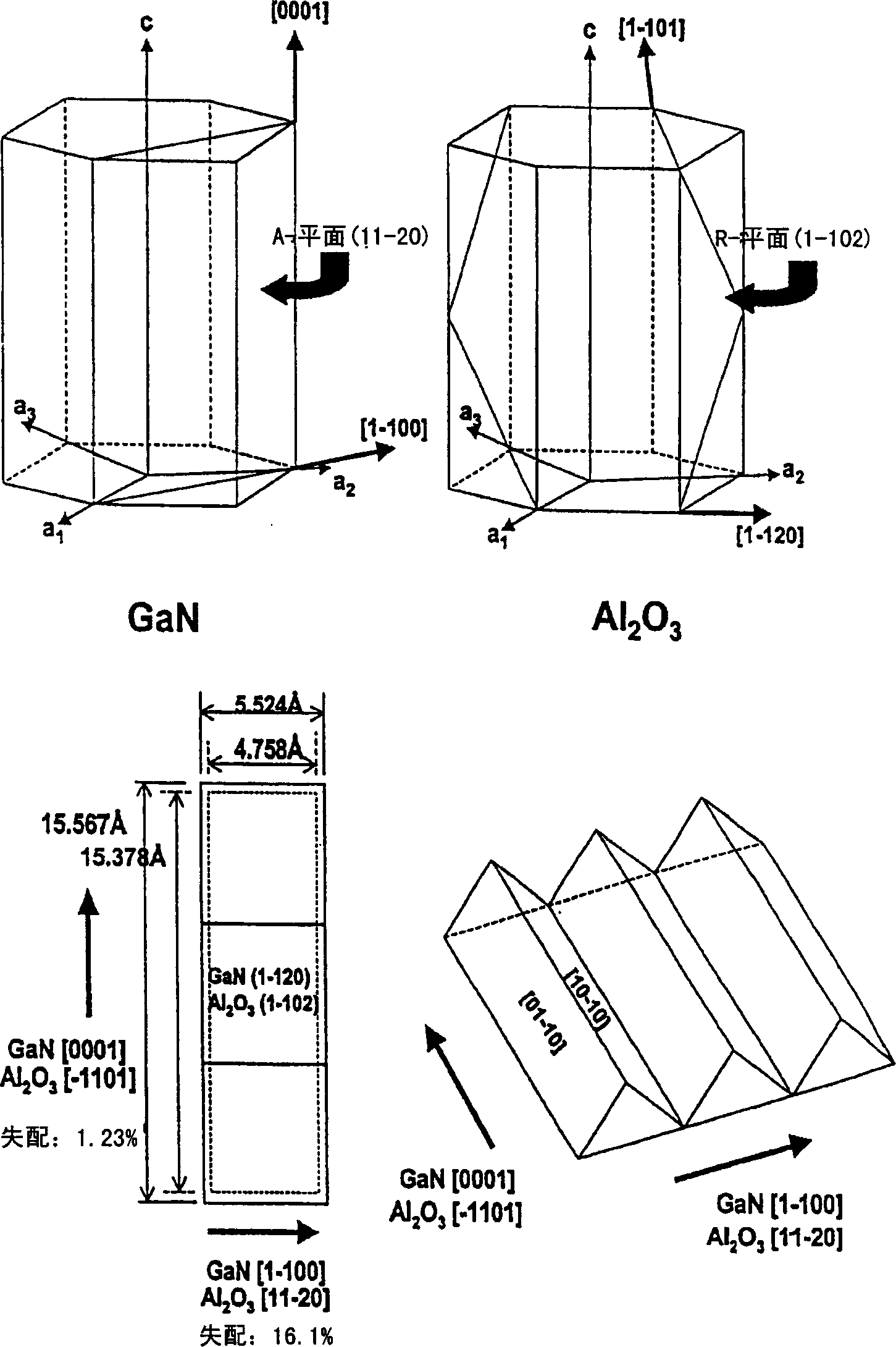
[0037] In the HVPE reactor, a single-crystal r-plane sapphire substrate with a diameter of 50.8 mm was placed, and nitriding was performed at 950 to 1100° C. with gaseous ammonia, a gas mixture of ammonia and hydrogen chloride, and gaseous ammonia in sequence.

[0038] On the nitride substrate thus obtained, a gallium nitride single crystal film was allowed to grow at a rate of 75 µm / hr by bringing gaseous gallium chloride and gaseous ammonia into contact therewith at 1000°C. Gallium chloride gas and gaseous ammonia, produced by the reaction of gallium with hydrogen chloride, are introduced through two separate inlets at a volume ratio of gaseous hydrogen chloride: gaseous ammonia of 1:6. The reactor chamber is maintained at a temperature in the range of 600 to 900°C at ambient pressure. Growth of the gallium nitride single crystal film was performed for 400 minutes to form a 500 μm thick gallium nitride semiconductor film on the substrate.

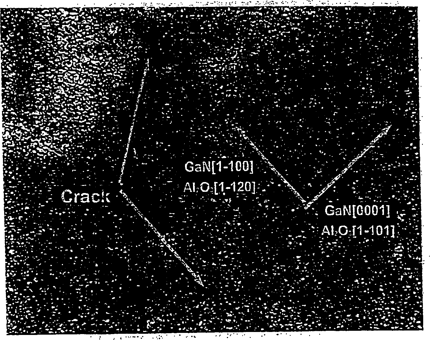
[0039] Figure 4 and 5 A photog...

example 2

[0043] Except that the volume ratio of gaseous hydrogen chloride and gaseous ammonia is in the range of 1:2-5, the steps of Example 1 are repeated to form a 500 μm thick gallium nitride semiconductor film on a sapphire substrate.

[0044] Figure 8A and 8B SEM photographs and XRD vibration curves of the surface of the thus formed a-plane GaN thick film are shown respectively. Figure 8B The XRD vibrational curve of the a-plane nitride film has a FWHM value of 342 arc seconds, which is the smallest value among the FWHM values ​​reported so far, which indicates that the crystallinity of the film is significantly improved.

[0045] As described above, according to the method of the present invention, a high-quality nonpolar single-crystal a-face nitride semiconductor wafer without voids, warpage, or cracks can be produced quickly and efficiently, and it can be advantageously used for LED manufacturing in the substrate.


PUM

PropertyMeasurementUnit
thicknessaaaaaaaaaa
thicknessaaaaaaaaaa
thicknessaaaaaaaaaa

Abstract

A single crystalline a-plane nitride semiconductor wafer having no voids, bending or cracks can be rapidly and effectively prepared by hydride vapor phase epitaxy (HVPE) growth of the a-plane nitride semiconductor film on a single crystalline r-plane sapphire substrate at a temperature ranging from 950 to 1,100 DEG C and at a rate ranging from 30 to 300 mu m / hr.

Description

technical field [0001] The invention relates to a non-polar single crystal a-plane nitride semiconductor wafer without voids, warpage or cracks and a method for preparing the nitride semiconductor wafer. Background technique [0002] Single-crystal nitride-based wafers used as substrates in the manufacture of semiconductor devices are mainly c-plane ({0001} plane) thin films grown on c-plane sapphire substrates by conventional methods and then separated from them. Methods such as Metal Organic Chemical Vapor Deposition (MOCVD), Molecular Beam Epitaxy (MBE) and Hydride Vapor Phase Epitaxy (HVPE). [0003] However, such a c-plane nitride film grown on a c-plane sapphire substrate is prone to cracks due to differences in lattice parameters and thermal expansion coefficients at the interface during growth. In the case where the c-plane nitride film is doped with an element such as silicon, this crack problem is even more serious. Also, c-plane nitride films, such as GaN / AlGaN ...

Claims


Application Information

Patent Timeline
Patent Type & Authority Applications(China)
IPC IPC(8): C30B29/38C23C16/34C30B25/02C30B25/18C30B29/40H01L21/205
CPCC30B25/18C30B29/403C30B25/02H01R13/4532
Inventor 申铉敏李惠龙李昌浩金贤锡金政敦孔善焕
Owner SAMSUNG CORNING PRECISION MATERIALS CO LTD
Why Eureka
Try Eureka