Method of manufacturing circuit device
A manufacturing method and circuit device technology, which can be applied in circuit devices, printed circuit manufacturing, circuits, etc., can solve problems such as miniaturization of difficult circuit devices, and achieve the effects of improved weight reduction, improved heat dissipation, and reduced manufacturing processes
- Summary
- Abstract
- Description
- Claims
- Application Information
AI Technical Summary
Problems solved by technology
Method used
Image
Examples
no. 1 approach
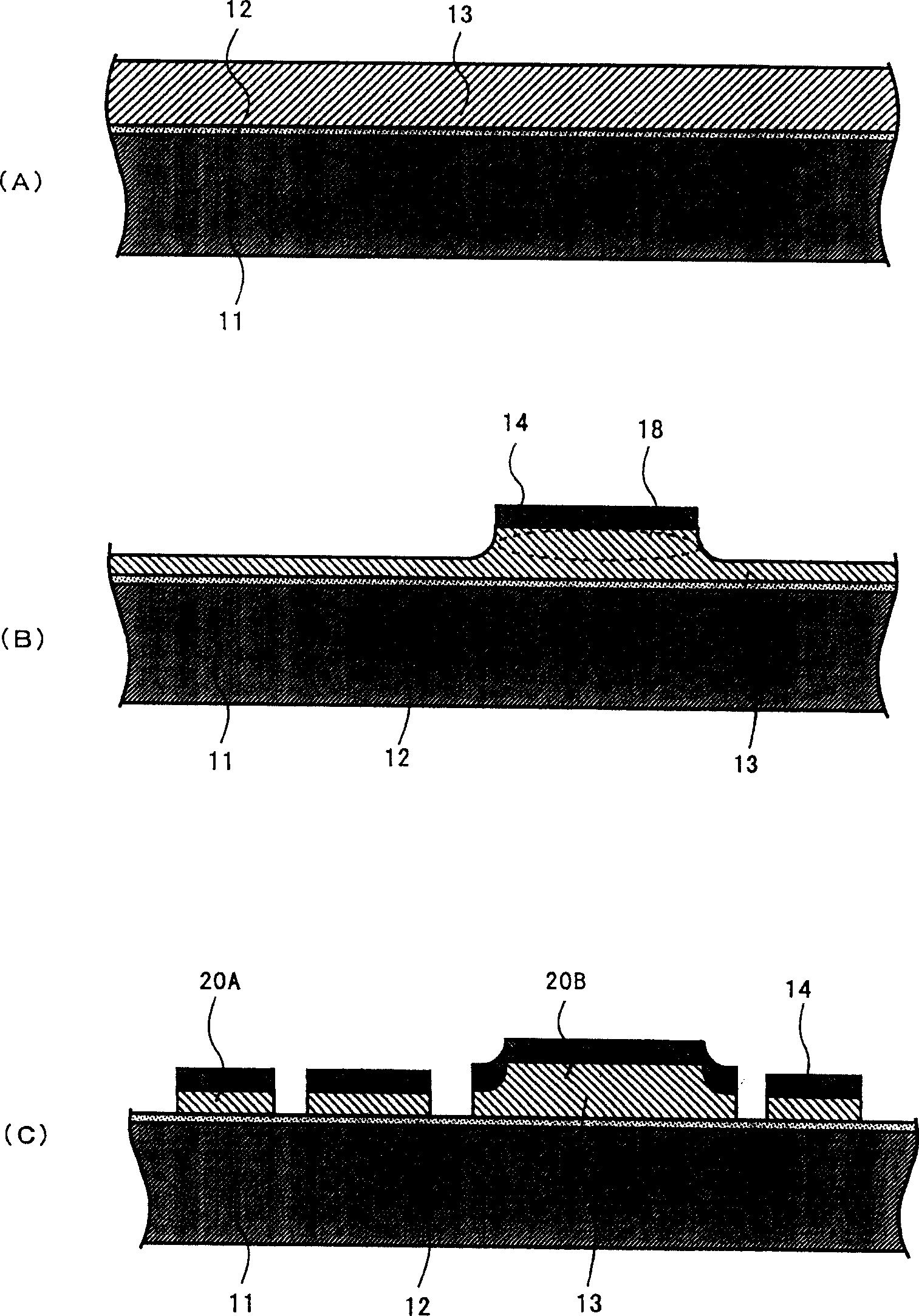
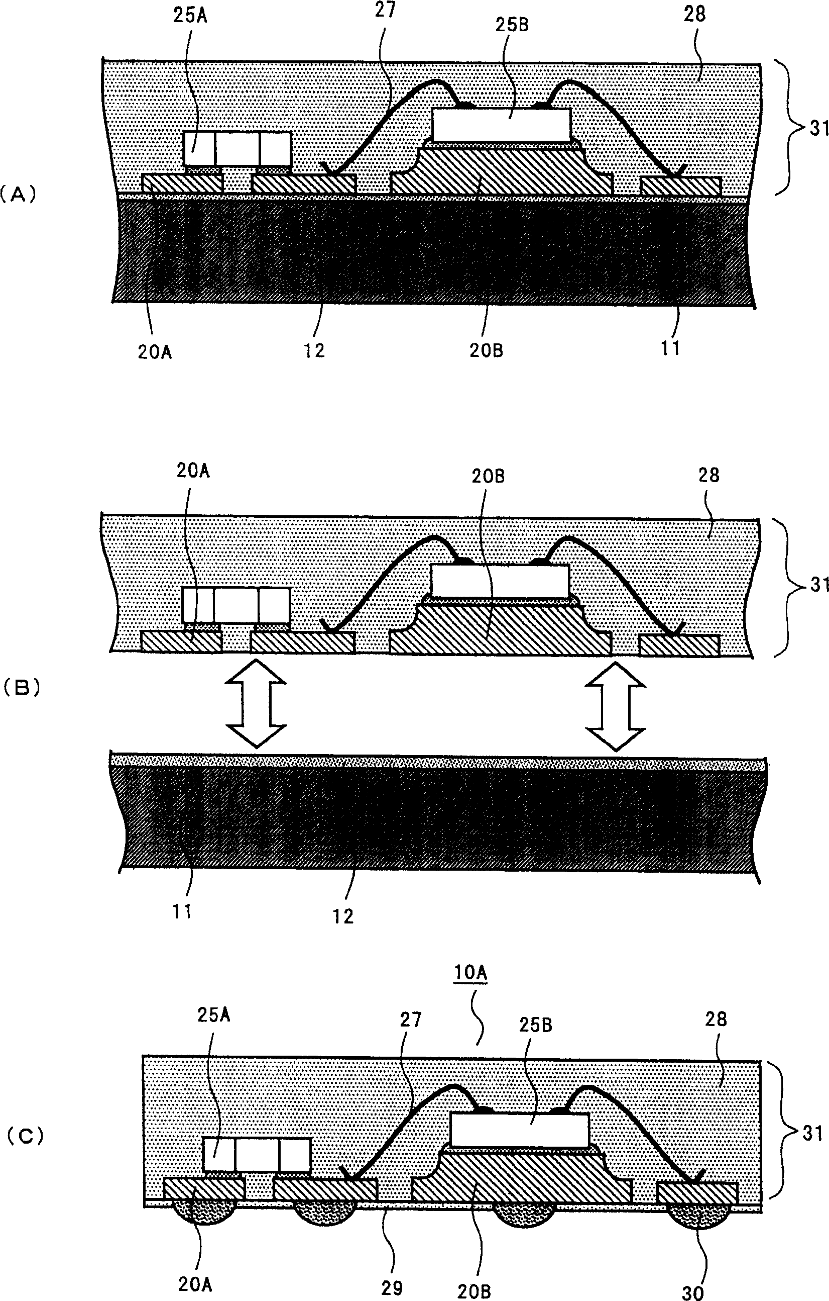
[0029] refer to figure 1 and figure 2 A method of manufacturing the circuit device according to the first embodiment will be described.
[0030] First, refer to figure 1 (A), the conductive foil 13 is pasted on the support substrate 11 via the adhesive 12 . The material of the conductive foil 13 is selected in consideration of solder adhesion, bonding, and plating properties. As a specific material, a conductive foil made of Cu as a main raw material, a conductive foil made of Al as a main raw material, or a conductive foil made of an alloy such as Fe—Ni, or the like is used. In addition, other conductive materials are also possible, and etchable conductive materials are particularly preferred. The thickness of the conductive foil 13 is about 10 μm to 300 μm. However, a conductive foil of 10 μm or less or 300 μm or more may be used.
[0031] As the adhesive 12, a thermoplastic resin, a UV sheet (substance that loses adhesiveness by irradiating ultraviolet rays), or th...
no. 2 approach
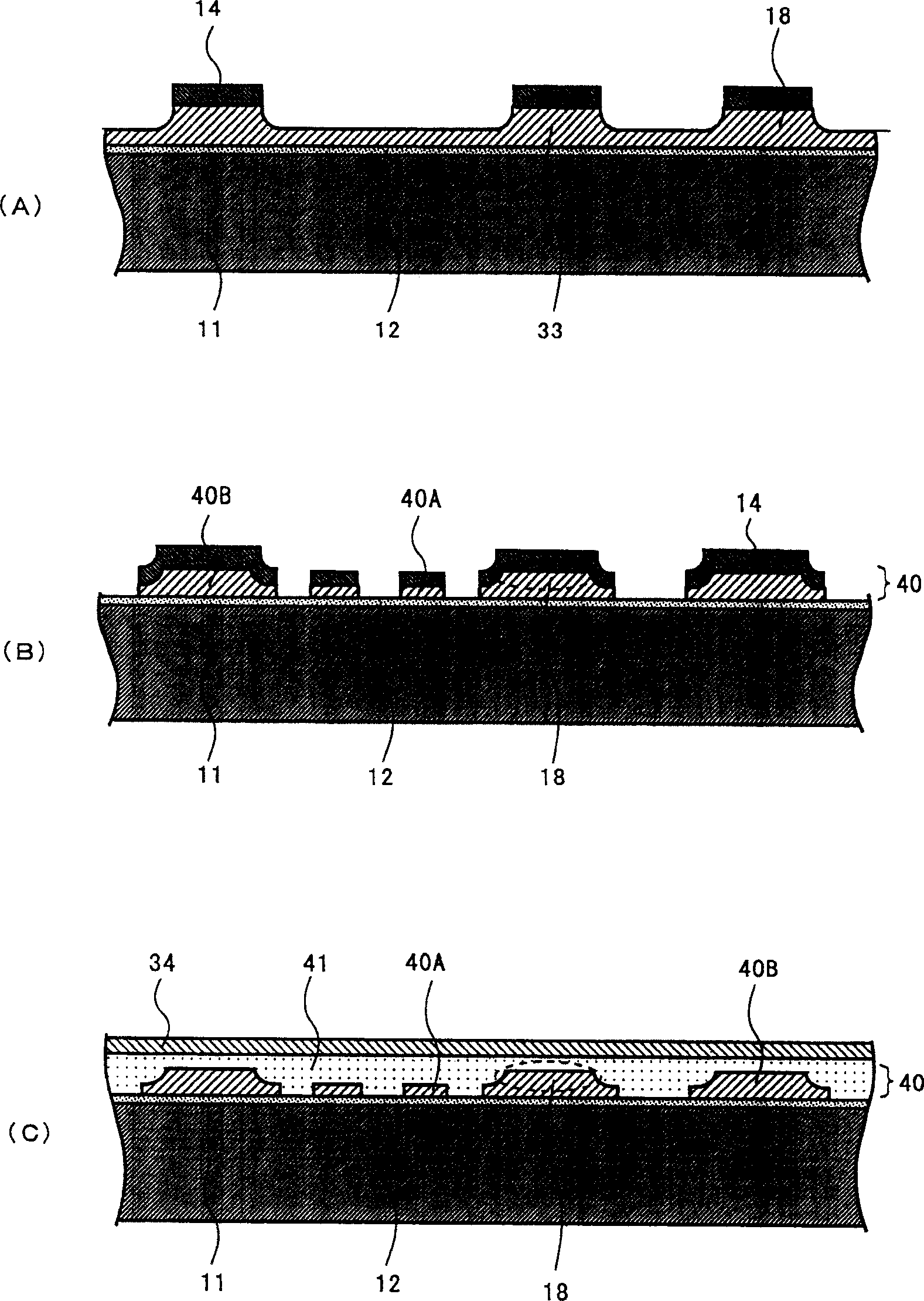
[0050] refer to Figure 3 ~ Figure 5 A method of manufacturing the circuit device according to the second embodiment will be described. The basic steps of the manufacturing method of the circuit device of this embodiment are the same as those of the first embodiment. Therefore, a description will be given here centering on the differences.
[0051] First, refer to image 3 (A), the protrusions 18 are formed on the first conductive film 33 bonded with the adhesive 12 on the support substrate 11 . The first conductive film 33 is half-etched using the resist 14 as a mask to form the protruding portion 18 which is a thick portion and a thin portion. After the protrusions 18 are formed, the resist 14 is removed.
[0052] refer to image 3 (B), same as the previous embodiment, etch the thin part to form a thick conductive pattern and a thin conductive pattern. Here, the resist 14 is patterned so as to cover a region wider than the region of the convex portion 18 . Then, wet e...
PUM
 Abstract
Description
Claims
Application Information


