Gallium nitride based LED chip and its manufacturing method

A light-emitting diode, gallium nitride-based technology, applied in electrical components, circuits, semiconductor devices, etc., can solve the problems of increasing chip temperature, affecting the reliability and life of the chip, and improving the working current and input power. , The effect of improving the current diffusion and improving the heat dissipation capacity

Inactive Publication Date: 2006-02-22
东莞市福地电子材料有限公司
View PDF0 Cites 43 Cited by
  • Summary
  • Abstract
  • Description
  • Claims
  • Application Information

AI Technical Summary

Problems solved by technology

The P-type contact electrode of the gallium nitride-based light-emitting diode chip generally used today is a whole. When the chip area is large, even if a more advanced comb-shaped electrode is used, the current diffusion performance is not good. In the P-type area and the N The place where the type area is close to is prone to the current concentration effect, which affects the increase of the working current density of the chip. In addition, the sapphire substrate of the gallium nitride-based light-emitting diode chip has poor thermal conductivity, which makes it difficult to transfer the heat generated when the chip is working. When the power increases, the temperature of the chip will rise, which will affect the reliability and life of the chip
At the same time, when the chip area is large, the P-type contact electrodes connected as a whole will also cause the so-called "waveguide effect", which will limit the light generated by the light-emitting active area to the chip, reducing the light output efficiency of the chip
[0003] In the prior art, the light-emitting active region, the P-type contact layer, and the P-type contact electrode of the gallium nitride-based light-emitting diode chip are all integrated, which does not involve the structure and structure of the corresponding array flip-chip gallium nitride-based light-emitting diode chip. Manufacturing method

Method used


Image

  • Gallium nitride based LED chip and its manufacturing method
  • Gallium nitride based LED chip and its manufacturing method
  • Gallium nitride based LED chip and its manufacturing method

Examples


Embodiment Construction

[0022] In order to further illustrate the content of the present invention, the present invention will be described in detail below in conjunction with the examples.

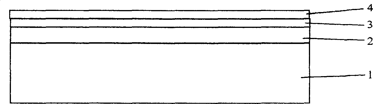
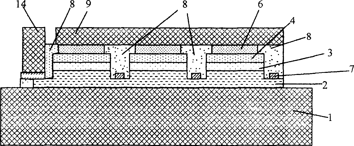
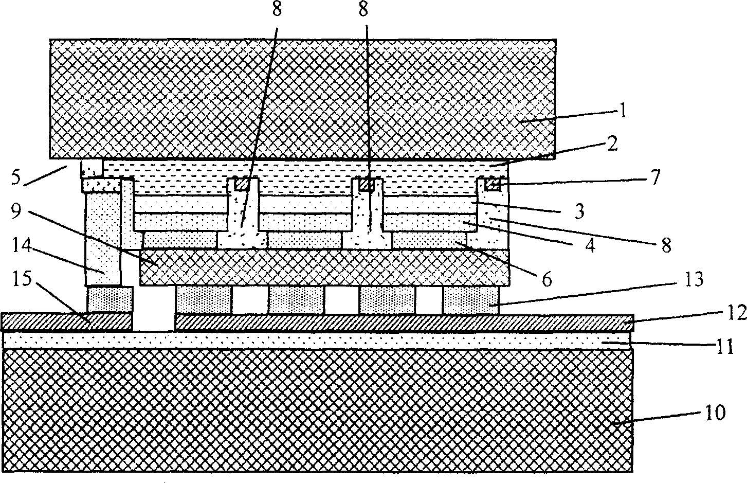
[0023] refer to image 3 , in the gallium nitride-based light-emitting diode chip shown, a sapphire substrate 1 with a thickness between 70 microns and 150 microns (such a thickness has both good light transmission and relatively good manufacturability) is set There is an N-type contact layer 2, and stacked light-emitting active regions 3, P-type contact layers 4 and P-type contact electrodes 6 are discretely arrayed on the N-type contact layer 2, and each group of light-emitting active regions 3, P-type The contact layer 4 and the P-type contact electrode 6 form an array unit, and the N-type contact electrode 7 of grid structure encloses each array unit in a grid. General array element linearity (circular linearity refers to the length of diameter, ellipse linearity refers to the length of long diameter, trian...


PUM

PropertyMeasurementUnit
thicknessaaaaaaaaaa
thicknessaaaaaaaaaa
thicknessaaaaaaaaaa

Abstract

The invention discloses a gallium nitride light-emitting diode and its manufacturing method. Wherein, the light-emitting active region 3, P contact layer 4, P contact electrode 6 discrete array are arranged on the N contact layer 2; the N contact electrode 7 is arranged as net structure; by face-down bonding technique and the welded material protruded block 13 of tube corn supporter, the P electrode thickened metallic layer 9 is connected to the contact electrode layer 12 of P region and the N electrode thickened reflective metallic layer 14 is connected to the contact electrode layer 15 of N region; the contact electrode layer 12 of P region and the contact electrode layer 15 of N region are arranged on the isolated layer 11 which is over the substrate 10 of tube corn supporter. First, processing the epitaxial sheet of gallium nitride light-emitting diode into the body of tube corn; then, forming the tube corn supporter on the substrate of tube corn supporter; at last, connecting the body of tube corn with the tube corn supporter by the technique of face-down bonding. Said invention can improve the luminous efficiency, the diffusion of current, and increase the heat conductance.

Description

technical field [0001] The invention belongs to the technical field of semiconductor optoelectronics, in particular to a product of a gallium nitride-based light-emitting diode chip and a manufacturing method thereof. Background technique [0002] Gallium nitride (GaN)-based compound semiconductors and their quantum well structure light-emitting diodes (LEDs) have the advantages of high reliability, high efficiency, long life, full solidification, and low power consumption. There is a huge application market in the field of general light display and indication, especially the combination of gallium nitride-based purple or blue light-emitting diodes and phosphors can be made into white light diodes, which has a potential application market in the lighting field and is expected to replace the current incandescent lamps in the future And fluorescent lamps, become the green lighting source in the 21st century. The P-type contact electrode of the gallium nitride-based light-emit...

Claims


Application Information

Patent Timeline
Patent Type & Authority Applications(China)
IPC IPC(8): H01L33/00
Inventor 李炳乾李炳田
Owner 东莞市福地电子材料有限公司
Why Eureka
Try Eureka