Method for manufacturing semi-transparent semi-reflective electrode substrate, reflective element substrate, method for manufacturing same, etching composition used for the method for manufacturing th

A semi-transmissive, semi-reflective, electrode substrate technology, applied in the field of etching solution, can solve the problems of complex manufacturing process, difficult viewing, different viewing methods, etc., and achieve the effect of shortening the manufacturing time

Inactive Publication Date: 2006-03-08
IDEMITSU KOSAN CO LTD
View PDF6 Cites 9 Cited by
  • Summary
  • Abstract
  • Description
  • Claims
  • Application Information

AI Technical Summary

Problems solved by technology

[0009] However, for transflective liquid crystals, reflective electrodes and transmissive electrodes need to be provided in the same pixel in the electrode part for liquid crystal driving, and there are complicated manufacturing processes, lower yields, and higher prices, as well as differences between transmissive and reflective modes. It is not easy to watch due to different viewing methods

Method used


Image

  • Method for manufacturing semi-transparent semi-reflective electrode substrate, reflective element substrate, method for manufacturing same, etching composition used for the method for manufacturing th
  • Method for manufacturing semi-transparent semi-reflective electrode substrate, reflective element substrate, method for manufacturing same, etching composition used for the method for manufacturing th
  • Method for manufacturing semi-transparent semi-reflective electrode substrate, reflective element substrate, method for manufacturing same, etching composition used for the method for manufacturing th

Examples


Embodiment 1-1

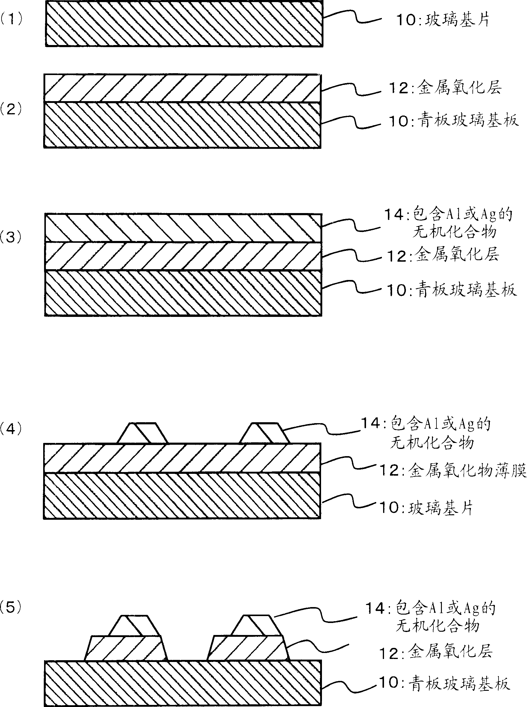
[0142] First, the metal oxide layer 12 is coated with SiO 2 The blue plate glass (soda lime glass) substrate 10 (refer to figure 1 (1)) on the film. The status is shown in figure 1 (2). In addition, in forming the metal oxide layer 12, a DC magnetron sputtering apparatus (manufactured by Shinko Seiki Co., Ltd.) was used.

[0143] In addition, the temperature of the blue glass substrate 10 at the time of film formation was 200 degreeC. In addition, the film thickness of the formed metal oxide layer 12 was 75 nm, and the resistivity was 380 μΩcm.

[0144] Next, the inorganic compound layer 14 was formed on the metal oxide layer 12 using a target Ag composed of Ag—Pd—Cu (98.5:0.5:1.0% by weight). In addition, the film thickness of the inorganic compound layer 14 was 100 nm. Its form is shown in figure 1 (3). In addition, the metal oxide layer 12 and the inorganic compound layer 14 mainly composed of Ag are referred to as an electrode layer. In addition, in Figure 1~...

Embodiment 1-2

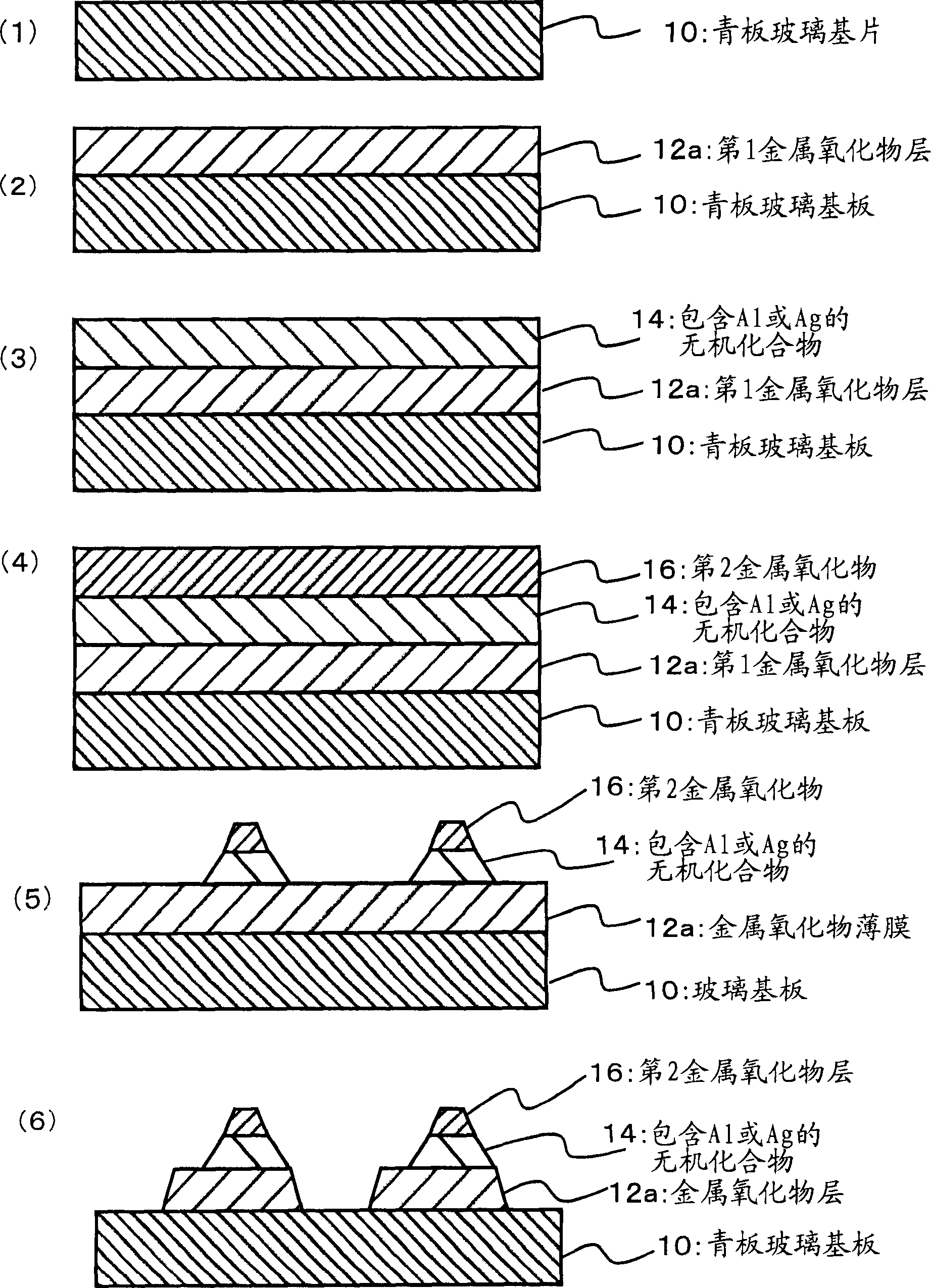
[0157] A second target comprising indium oxide-tin oxide-cerium oxide (In / (In+Sn)=90 atomic%, Ce / (In+Sn+Ce)=4.9 atomic%) was used instead of the target used in Example 1-1. first target. In addition, Ag-Au-Ni (98.5:0.5:1.0 wt%) was used instead of Ag-Pd-Cu (98.5:0.5:1.0 wt%) used in Example 1-1. Other than that, it carried out by the same method as Example 1-1. That is, film formation of the first metal oxide layer 12 a and the inorganic compound layer 14 is performed. This form is shown in figure 2 (1) ~ (3). Furthermore, the first metal oxide layer 12a formed in the present embodiment 1-2, that is, as figure 2 The first metal oxide layer 12a shown in (2) is and figure 1 The metal oxide layer 12 shown in (2) is the same metal oxide layer.

[0158] Next, the second metal oxide layer 16 was formed using a third target containing indium oxide+zinc oxide (In / (In+Zn)=75 atomic %) as a protective film. In addition, the temperature at the time of film formation was room te...

Embodiment 1-3

[0164] A fourth target of indium oxide-tin oxide-praseodymium oxide (In / (In+Sn)=90 atomic%, Pr / (In+Sn+Pr)=4.6 atomic%) was used instead of the one used in Example 1-1 first target. Other than that, the metal oxide layer 12 and the inorganic compound layer 14 were formed in the same manner as in Example 1-1.

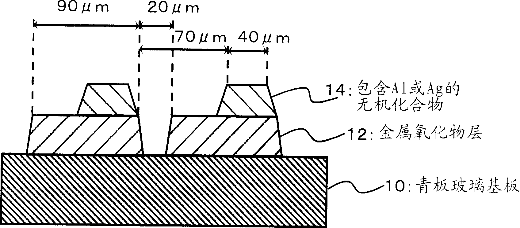
[0165] Next, etching was performed in the same manner as in Example 1-1 to manufacture a transflective electrode substrate. The resistivity of the metal oxide layer 12 was 450 μΩcm. This form is shown in figure 1 (1)~(5) of.

[0166] The thus obtained semi-transmissive and semi-reflective electrode substrate can achieve low resistance. In addition, when the substrate surface was observed with a scanning electron microscope, the surface roughness of the metal oxide layer 12 was not observed. In addition, almost no change was seen in the edge portion of the inorganic compound layer 14 before and after etching with oxalic acid. This means that the etchant σ of oxalic ...


PUM

PropertyMeasurementUnit
thicknessaaaaaaaaaa
thicknessaaaaaaaaaa
thicknessaaaaaaaaaa

Abstract

An etchant for selective etching is used to simplify the production process of a semi-transparent semi-reflective electrode substrate, and temporal loss is not produced by avoiding troublesome repeated works, thereby efficiently providing a semi-transparent semi-reflective electrode substrate. A method for manufacturing a semi-transparent semi-reflective electrode substrate where a metal oxide layer (12) made of at least indium oxide and an inorganic compound layer (14) at least made of Al or Ag are formed in order of mention. The method comprises a step of etching the inorganic compound layer (14) with an etchant lambda composed of phosphoric acid, nitric acid, and acetic acid and a step of etching the metal oxide layer (12) with an etchant sigma containing oxalic acid.

Description

technical field [0001] The invention relates to a method for manufacturing a transflective and semireflective liquid crystal electrode substrate. It also relates to an etchant used in the manufacture of a transflective electrode substrate. [0002] Also, the present invention relates to a reflective electrode substrate in a reflective liquid crystal or a light-emitting element, a method for producing the same, and an etching solution used in the method for producing the same. Background technique [0003] One of the existing technologies (semi-transmissive and semi-reflective liquid crystal) [0004] Hitherto, research and development of transflective liquid crystals have been vigorously conducted for the reasons described below. [0005] (1) Since it is semi-transmissive and semi-reflective, a bright display can be obtained regardless of whether it is outdoors or indoors. [0006] (2) When used in a bright place, it can be used as a reflection type, so power consumption ...

Claims


Application Information

Patent Timeline
Patent Type & Authority Applications(China)
IPC IPC(8): H01L21/308H05B33/26G02F1/1343G02F1/1335H01B13/00
Inventor 井上一吉
Owner IDEMITSU KOSAN CO LTD
Why Eureka
Try Eureka