Forming electromagnetic communication circuit components using densified metal powder

A metal powder and integrated circuit technology, applied in the direction of circuits, printed circuits, electrical components, etc., can solve the problems of reducing the total conductivity of circuit patterns, weak conductors of circuits, etc., and achieve the minimum process cost and pollution, easy recycling, and low cost Effect

Inactive Publication Date: 2006-04-05
3M INNOVATIVE PROPERTIES CO
View PDF3 Cites 6 Cited by
  • Summary
  • Abstract
  • Description
  • Claims
  • Application Information

AI Technical Summary

Problems solved by technology

[0003] Adhesives and organic binders in these compounds are weak conductors of circuits and, wh

Method used


Image

  • Forming electromagnetic communication circuit components using densified metal powder
  • Forming electromagnetic communication circuit components using densified metal powder
  • Forming electromagnetic communication circuit components using densified metal powder

Examples


Embodiment 1

[0083] This example illustrates the calculation of a sample figure of merit (FOM). Using %FOM, for pure copper, the measured resistance of the pressed powder pattern compared to the smallest possible theoretical resistivity satisfies the following equation:

[0084] %FOM=(R theoretical / R measured )×100

[0085] where R theoretical is the resistivity of pure copper, and R is calculated from the measured resistance of the sample pressed powder pattern measured .

[0086] The density of solid copper is 8.96g / cm 3 . The resistivity of copper is 1.73×10 -6 Ohm-centimeter (ohms-cm). For the mass and profile of the sample, for normalization, the mass (grams) per unit length (cm) and the resistance (ohms) per unit length (cm) are plugged into the FOM equation such that:

[0087] %FOM=(R theoretical / R measured )×100

[0088] where: R theoretieal =(Copper Density)(Copper Resistivity)=0.0000155g-ohm / cm 2

[0089] R measured =[(mass in grams per centimeter)(per centimete...

Embodiment 2

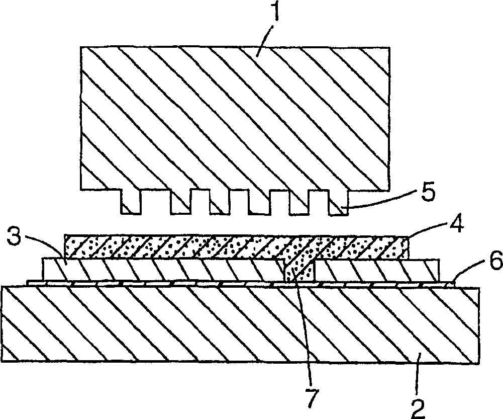
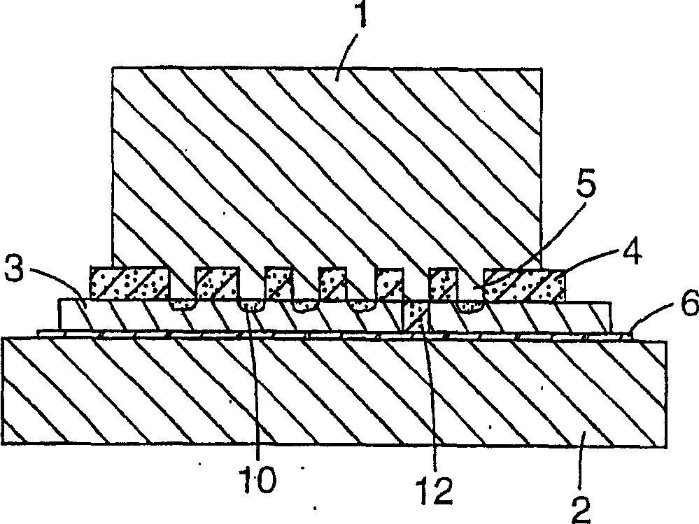
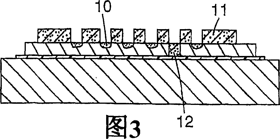
[0094] Copper powder (dendritic, 3 microns, 99.7%) from Sigma-Aldrich (Milwaukee WI) was cleaned by stirring it in a solution of hydrochloric acid containing 10% water, followed by 1 water rinse and 3 ethanol rinses. The copper powder can be air dried for approximately 1 hour. A 20 cm diameter #270 molecular sieve was placed over a 20 cm diameter, 46 cm long cardboard tube. Cardboard tubes were placed over seven sets of 55 cm diameter model 54 Whatman filter paper circles. Tin powder (AEE 1-5 micron 99.9%), then copper powder was sprayed on molecular sieves and allowed to settle on the filter paper to a depth varying from about 0.1 mm to 0.5 mm for each sample. In the following examples, this method of applying one or more metal powders to a substrate is referred to as a sieving method.

[0095] In a first step, the patterned mold was pressed onto the powder by applying 27 megapascals (MPa) on the powder and filter paper using a Carver platen press (Model 3891, Wabash, India...

Embodiment 3-8

[0099] Examples 3-8 were prepared using the sieving method of Example 2. In one step, metal powder was captured into a pattern and densified by pressing a patterned die onto the powder at the pressures shown in Table 1. As shown in Table 1, two different paperboards and combinations of metal powder and particle types were used. The resistance of each sample was measured and Table 1 shows the calculated %FOM.

[0100] Table 1 shows the results using combinations of substrates and metal powders under different condition sets. Table 2 shows abbreviations for substrates and metals.


PUM


Abstract

Manufacturing techniques are described for forming electrical components. For example, a layer of a metal powder composition is deposited onto at least a portion of a substrate. Pressure is applied to the metal powder composition by hydraulic press that has one or more projections in order to capture a pattern on the substrate. The metal powder composition compressed by the projections of the hydraulic press adhere to the substrate to form the captured pattern. The metal powder composition in regions not compressed by the projections of hydraulic press do not adhere to the substrate and may be removed. The metal powder composition may be compressed to form electrical components, such as antennae, capacitor plates, conduction pads and the like, for use in an electronic surveillance system (EAS), a radio frequency identification (RFID) system, or the like.

Description

technical field [0001] This application relates to electronic articles formed from metal powder compositions and methods of making the same. Background technique [0002] Patterned metal articles such as printed circuit boards are widely used in the electronics industry. Printed circuits can be fabricated by applying pressure to metal particles on an adhesive-coated substrate using a heated die. Metal particles can also be mixed with a cured organic binder and provided to the substrate using an adhesive layer, heat and pressure. Printed circuits can also be fabricated by embedding conductive amorphous particles mixed with inorganic composite materials into heat-softenable substrates. Screen printing can also be used to provide a mixture of organic materials and conductive particles to a substrate, and compositions containing metal-organic compounds and metal particles can also be screen printed onto a substrate and heated to form circuit patterns. [0003] Adhesives and o...

Claims


Application Information

Patent Timeline
IPC IPC(8): H05K3/10G08B13/24G06K19/077G06K17/00G06K19/02G06K19/067G06K19/073
CPCG06K19/067G06K19/0739H05K3/102G06K19/07783G06K19/07758G06K19/07749G06K19/02G06K2017/0074G06K19/027G06K19/07779G06K2017/0045G06K19/0672H01L2224/83Y10T156/10Y10T428/24917H05K3/10
Inventor 大卫·W·库恩大卫·C·科斯肯迈基
Owner 3M INNOVATIVE PROPERTIES CO
Why Eureka
Try Eureka