Copper alloy thin films, copper alloy sputtering targets and flat panel displays
一种平板显示器、合金薄膜的技术,应用在溅射镀覆、仪器、薄料处理等方向,能够解决联结线路断裂、增加电阻率、影响联结线路可靠性等问题,达到满意可靠性、低电阻率的效果
- Summary
- Abstract
- Description
- Claims
- Application Information
AI Technical Summary
Problems solved by technology
Method used
Image

Examples
Embodiment 1
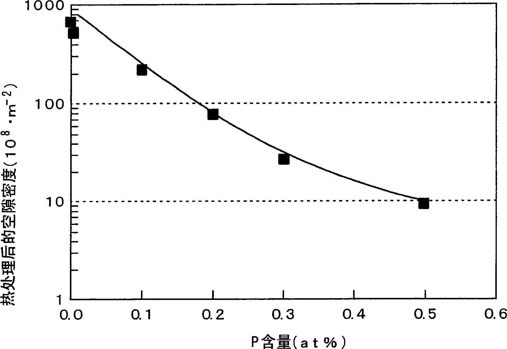
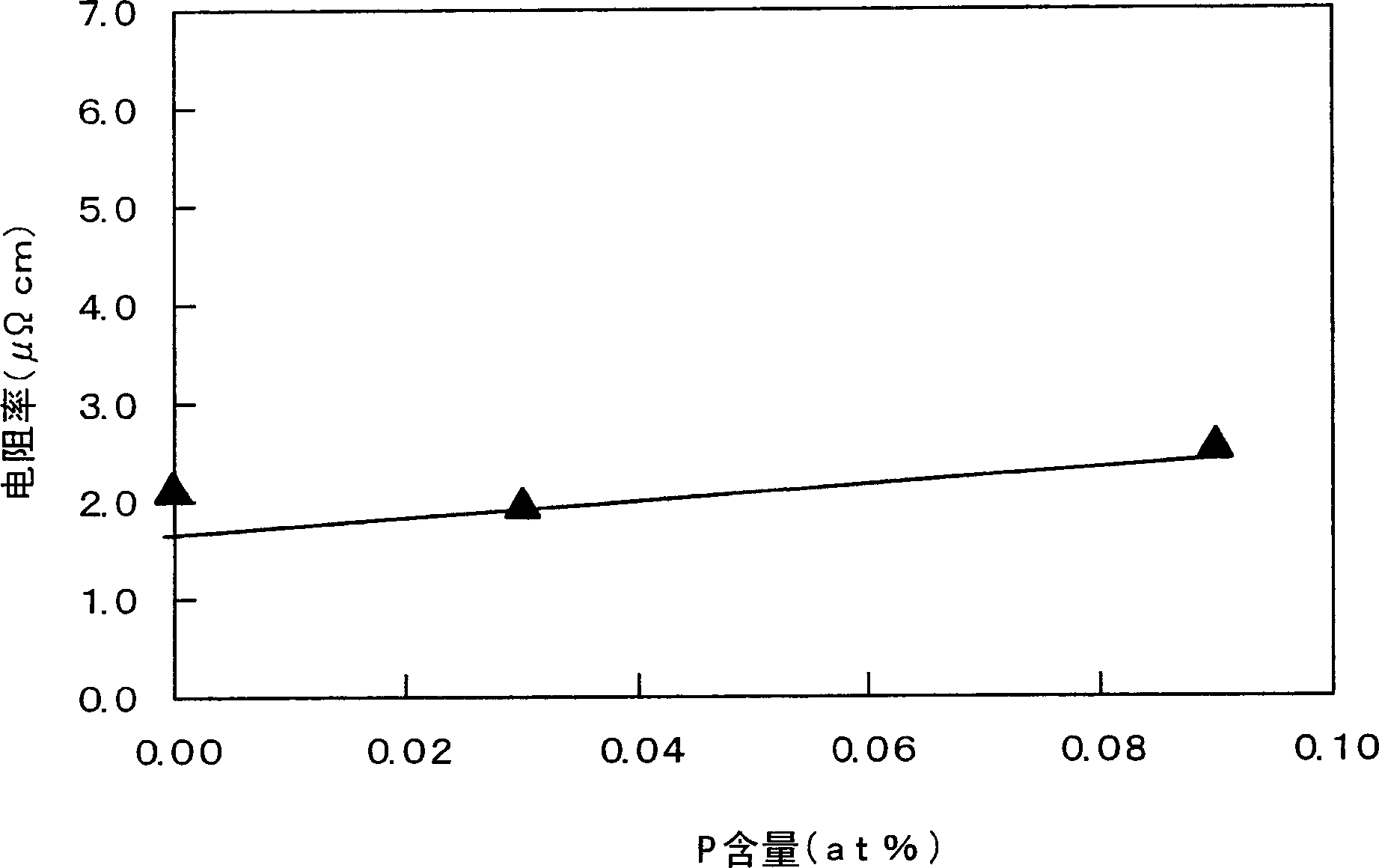
[0128] A sputtering target comprising a Cu alloy containing 0.28 atomic % Fe and 0.25 atomic % P with the balance being Cu and unavoidable impurities was prepared by a vacuum melting method. Using this sputtering target, a Cu-Fe-P alloy with a thickness of 300 nm was deposited on a glass substrate (#1737 glass from Corning Inc.) with a diameter of 50.8 mm and a thickness of 0.7 mm using a DC magnetron sputtering method film. The composition of the Cu-Fe-P alloy thin film was analyzed by inductively coupled plasma (ICP) atomic emission spectrometry, and it was found that the Fe content was 0.28 atomic % and the P content was 0.05 atomic %. At the time of film deposition, about 80% of P cannot be produced because P has a high vapor pressure.
[0129] Next, a pattern of a positive photoresist (thickness 1 μm) is formed on the Cu-0.28at%Fe-0.05at%P alloy film, etched with a mixed acid etchant, and the photoresist is removed with a photoresist remover. resist. A bond line patter...
Embodiment 2
[0132] A sputtering target comprising a Cu alloy containing 0.35 atomic % Co and 0.25 atomic % P with the balance being Cu and unavoidable impurities was prepared by a vacuum melting method. Using this sputtering target, a Cu-Co-P alloy with a thickness of 300 nm was deposited on a glass substrate (#1737 glass from Corning Inc.) with a diameter of 50.8 mm and a thickness of 0.7 mm using a DC magnetron sputtering method film. The composition of the Cu-Co-P alloy thin film was analyzed by inductively coupled plasma (ICP) atomic emission spectrometry, and it was found that the Co content was 0.35 atomic % and the p content was 0.05 atomic %. At the time of thin film deposition, since P had a high vapor pressure as in Example 1, about 80% of P could not be produced.
[0133] Next, form a pattern of a positive photoresist (thickness 1 μm) on the Cu-0.35at%Co-0.05at%P alloy film, etch with a mixed acid etchant, and remove the photoresist with a photoresist remover. resist. A bond...
Embodiment 3
[0136] A sputtering target comprising a Cu alloy containing 0.5 atomic % of Mg and 0.25 atomic % of P and the balance of Cu and unavoidable impurities was prepared by a vacuum melting method. Using this sputtering target, a Cu-Mg-P alloy with a thickness of 300 nm was deposited on a glass substrate (#1737 glass from Corning Inc.) with a diameter of 50.8 mm and a thickness of 0.7 mm using a DC magnetron sputtering method film. The composition of the Cu-Mg-P alloy thin film was analyzed by inductively coupled plasma (ICP) atomic emission spectrometry, and it was found that the Mg content was 0.5 atomic % and the p content was 0.05 atomic %. At the time of film deposition, as in Examples 1 and 2, about 80% of P could not be produced because P had a high vapor pressure.
[0137] Next, a pattern of a positive photoresist (thickness 1 μm) is formed on the Cu-0.5at%Mg-0.05at%P alloy film, etched with a mixed acid etchant, and the photoresist is removed with a photoresist remover. r...
PUM
| Property | Measurement | Unit |
|---|---|---|
| electrical resistivity | aaaaa | aaaaa |
| electrical resistivity | aaaaa | aaaaa |
| electrical resistivity | aaaaa | aaaaa |
Abstract
Description
Claims
Application Information
 - R&D
- Intellectual Property
- Life Sciences
- Materials
- Tech Scout
- Unparalleled Data Quality
- Higher Quality Content
- 60% Fewer Hallucinations
Browse by: Latest US Patents, China's latest patents, Technical Efficacy Thesaurus, Application Domain, Technology Topic, Popular Technical Reports.
© 2025 PatSnap. All rights reserved.Legal|Privacy policy|Modern Slavery Act Transparency Statement|Sitemap|About US| Contact US: help@patsnap.com