Process for producing gold surface pattern conductive polyphenylamine film

A conductive polyaniline, surface pattern technology, applied in electrolytic coatings, electrophoretic plating, electrolytic organic material plating, etc., can solve problems such as expensive equipment and damage to polymer layers, and achieve simple preparation methods, clear boundaries, and easy product composition. control effect

Inactive Publication Date: 2006-05-17
LANZHOU INST OF CHEM PHYSICS CHINESE ACAD OF SCI
View PDF0 Cites 4 Cited by
  • Summary
  • Abstract
  • Description
  • Claims
  • Application Information

AI Technical Summary

Problems solved by technology

Traditionally, the patterning of conductive polymers can be done by photolithography, electron beam etching, e

Method used


Image

  • Process for producing gold surface pattern conductive polyphenylamine film
  • Process for producing gold surface pattern conductive polyphenylamine film

Examples


Embodiment l

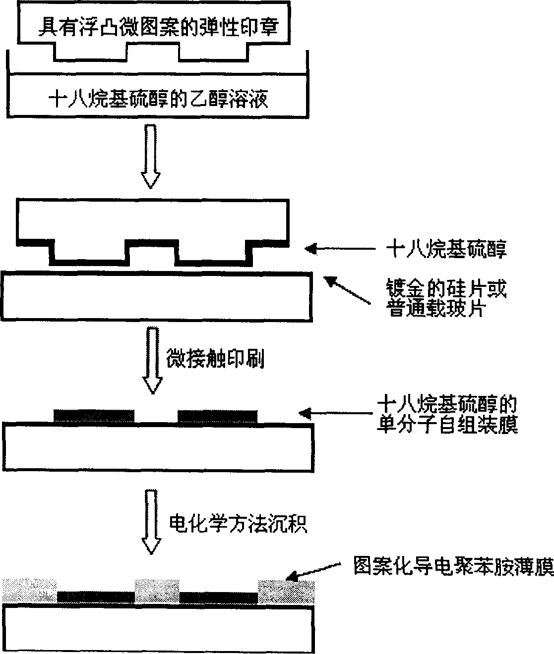
[0019] Fabrication of patterned polyaniline films on gold substrates:

[0020] 1. Preparation of Gold Substrate

[0021] The silicon substrate treated with the Piranha solution at 90° C. for half an hour was used to obtain a gold-plated substrate by vacuum thermal evaporation.

[0022] 2. Preparation of Patterned Elastic Stamps

[0023] Sylgard184 (Dow Corning Company) was coated on a micro-processed single-crystal silicon membrane plate, and then left to stand for 2 hours, cured at 150° C. for one hour, and an elastic stamp with micropatterns could be obtained after aging and peeling off.

[0024] 3. Fabrication of Patterned Self-Assembled Films

[0025] (1) A gold-plated silicon wafer was used as a substrate, and treated with a mixed solution (Piranha solution) of concentrated sulfuric acid and hydrogen peroxide with a volume ratio of 70%: 30% at 90° C. for 10 minutes.

[0026] (2) Prepare 2×10 -3 1 mole of octadecylmercaptan in absolute ethanol;

[0027] (3) immerse th...

Embodiment 2

[0033] Fabrication of patterned polyaniline films on gold-coated glass slide substrates:

[0034] 1. Preparation of Gold Substrate

[0035] The silicon substrate treated with the Piranha solution at 90° C. for half an hour was used to obtain a gold-plated substrate by vacuum thermal evaporation.

[0036] 2. Preparation of Patterned Elastic Stamps

[0037] The method is the same as above, peeled off after curing at 65°C for 90 minutes.

[0038] 3. Fabrication of Patterned Self-Assembled Films

[0039] (1) Using a patterned gold-plated glass slide as a working electrode, treat it with a mixed solution (Piranha solution) of concentrated sulfuric acid and hydrogen peroxide (Piranha solution) with a volume ratio of 70%: 30% at 85 ° C for 1 hour;

[0040] (2) Prepare 1×10 -3 1 mole of octadecylmercaptan in absolute ethanol;

[0041] (3) immerse the cleaned stamp in the prepared dilute mercaptan solution for 5 seconds, and dry it with nitrogen;

[0042] (4) Imprint the stamp ad...


PUM


Abstract

The present invention uses long-chain mercaptan and aniline which are easily adsorbed on gold surface as raw material, and adopts the following steps: firstly, making silicon wafer sample undergo the process of surface treatment, using photo-etching technique to form regular pattern on the silicon surface, using said template as mold, pouring Sylgard 184 on its patterned surface, solidifying and forming at proper temperature to form elastic stamp with relief structure; then utilizing vacuum thermal deposition process to obtain a gold layer with a certain thickness on the silicon wafer or general microslide, and utilizing microcontact printing method to form a patterned octodecamercaptan self-assembled film on the gold surface; finally, using electrochemical polymerization method to prepare patterned polyaniline film.

Description

technical field [0001] The invention relates to a method for preparing a patterned conductive polyaniline film on a gold surface. Background technique [0002] In recent years, the research on the patterning method of conductive polymers has attracted more and more attention. Patterned conductive polymers have many uses, such as making actuators, biosensors, and can replace metals in nano / micro-manufacturing to prepare integrated circuits (Science 2000, 290:1532. Adv. Mater. 2002, 14:1837). Traditionally, the patterning of conductive polymers can be done by photolithography, electron beam etching, etc. However, these methods not only require expensive equipment, but also may cause damage to the polymer layer. Therefore, microcontact printing technology has become very important as a non-lithographic patterning technology. Fabrication of patterned self-assembled monolayers by microcontact printing. It serves as a template for regioselective deposition and has a guiding eff...

Claims


Application Information

Patent Timeline
IPC IPC(8): C25D5/02C25D9/02C25D13/08
Inventor 陈淼张瑞
Owner LANZHOU INST OF CHEM PHYSICS CHINESE ACAD OF SCI
Why Eureka
Try Eureka