

Etchant and etching method
An etchant and etching technology, applied in the manufacture of electrical components, circuits, semiconductor/solid-state devices, etc., can solve the problems of poor insulation resistance, insufficient coverage, increased exposed area, etc., and achieve the effect of improving the etching function
- Summary
- Abstract
- Description
- Claims
- Application Information
AI Technical Summary
Problems solved by technology
Method used
Image

Examples
Embodiment 1~7 and
[0074] Embodiment 1~7 and reference example 1~6
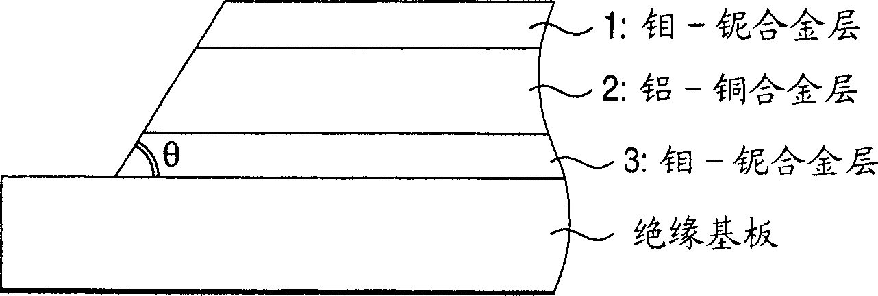
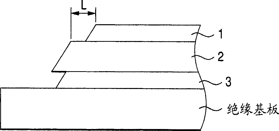
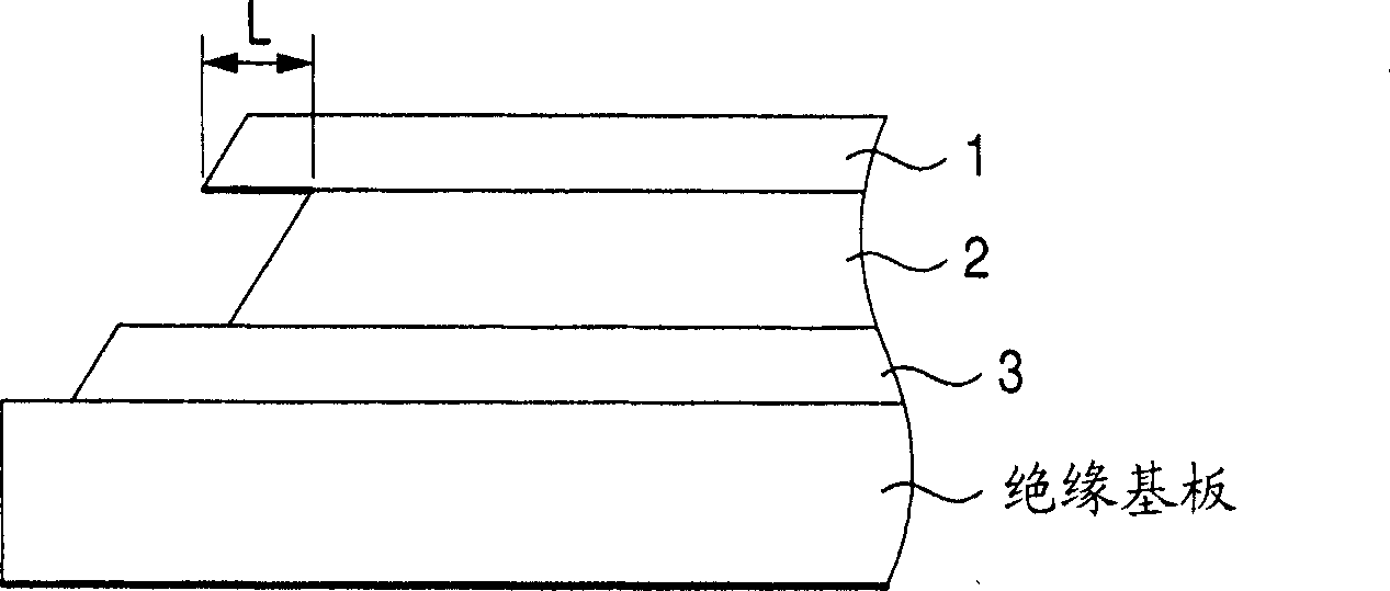
[0075] A molybdenum-niobium alloy layer (with a niobium content of 5% by weight) 3 with a thickness of 50 nm was deposited on the glass substrate by sputtering. AlCu (Al—Cu alloy; copper content: 5% by weight) was formed as an aluminum alloy layer 2 to a thickness of 300 nm by sputtering using argon gas on this layer. After that, the molybdenum-niobium alloy layer 1 having the same composition as above was continuously deposited to a thickness of 50 nm. Thus, forming as Figure 1A , Figure 1B and Figure 1C MoNb / AlCu / MoNb multilayer film shown.
[0076] A positive photoresist resin layer (about 1.5 μm in thickness) was further formed thereon by spin coating, and this layer was processed by photolithography to form a fine wiring pattern. The line width of this photoresist pattern is about 5 μm.
[0077] This substrate was cut into sheets having a width of about 10 mm and a length of 50 mm, and these sheets were used as etc...
PUM
| Property | Measurement | Unit |
|---|---|---|
| thickness | aaaaa | aaaaa |
Abstract
Description
Claims
Application Information