High power 650nm semiconductor laser for digital multi-purpose optical disks and manufacturing method

A manufacturing method and multi-functional technology, which can be applied to beam sources, optical recording heads, structures of active regions, etc., and can solve problems such as low practicability, high toxicity of drugs, and difficulty in meeting the requirements of fundamental mode output.

Inactive Publication Date: 2006-07-19
INST OF SEMICONDUCTORS - CHINESE ACAD OF SCI
View PDF0 Cites 9 Cited by
  • Summary
  • Abstract
  • Description
  • Claims
  • Application Information

AI Technical Summary

Problems solved by technology

[0013] 1. Large optical cavity structure and tapered cavity structure, but these structures are difficult to meet the requirements of fundamental mode output;
[0014] 2. The window structure with injection area, but it is difficult to manufacture, the cost is high, and it is easy to damage the laser structure;
[0015] 3. Chemical passivation, but the drugs required for passivation are very toxic and not very practical;

Method used


Image

  • High power 650nm semiconductor laser for digital multi-purpose optical disks and manufacturing method
  • High power 650nm semiconductor laser for digital multi-purpose optical disks and manufacturing method
  • High power 650nm semiconductor laser for digital multi-purpose optical disks and manufacturing method

Examples


Embodiment Construction

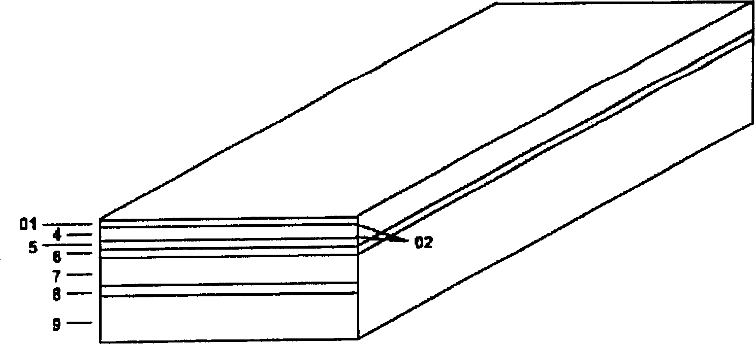
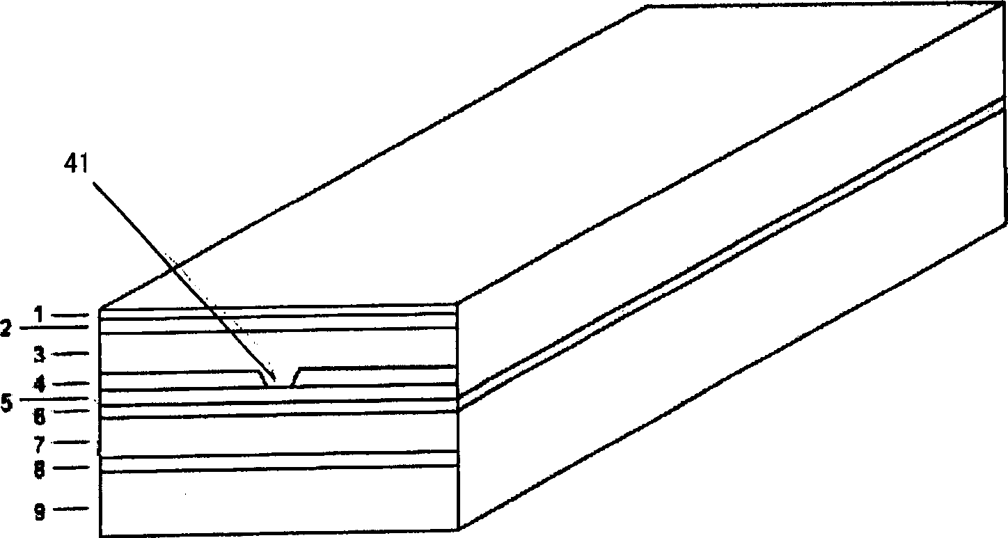
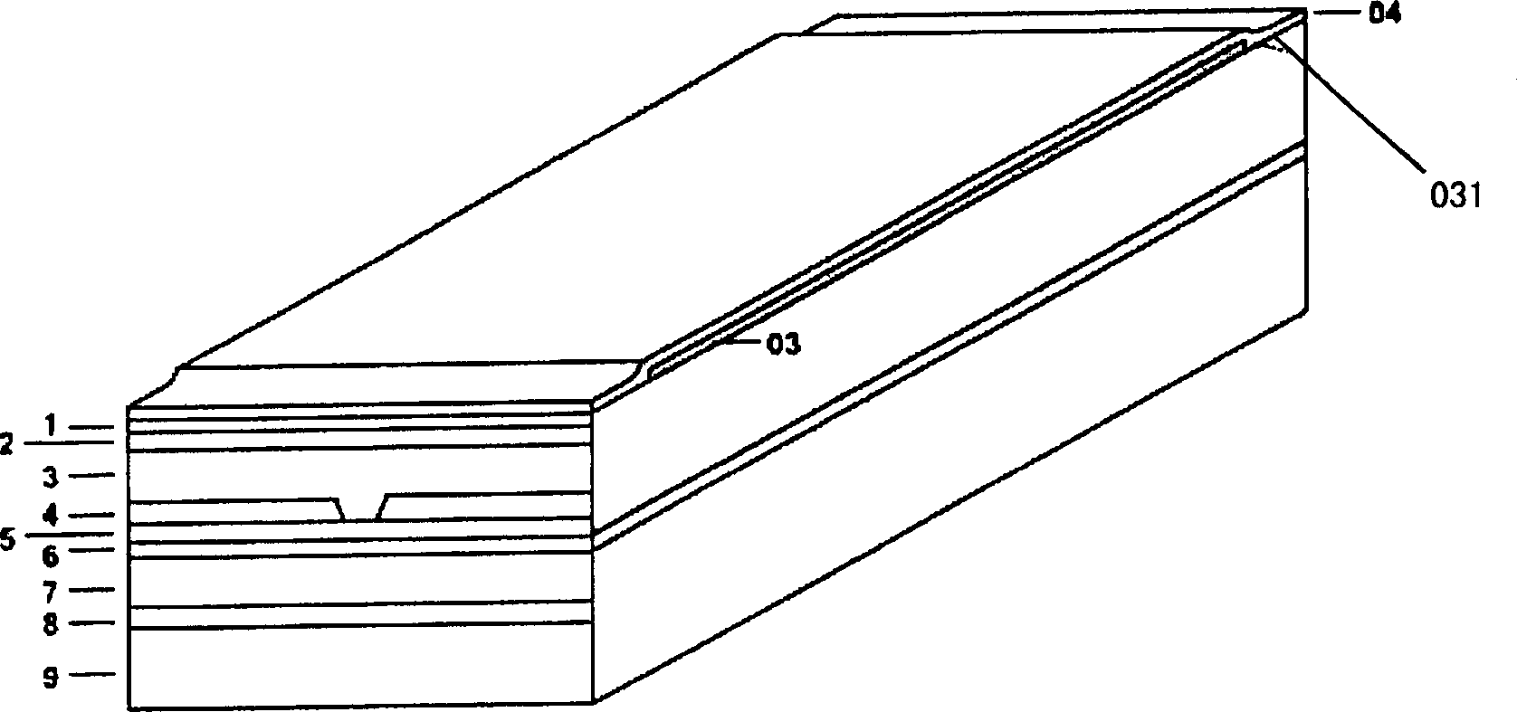
[0057] refer to Figure 5 and Figure 6 , a high-power 650nm semiconductor laser for a digital multifunctional disc of the present invention, comprising:

[0058] A substrate 9, the substrate 9 is used for epitaxial growth of the laser material structure thereon, the substrate is N-gallium arsenic on the (100) plane, and the (100) faces the A plane with an off-angle;

[0059] A buffer layer 8, which is fabricated on the substrate 9 to relieve the lattice mismatch between the substrate 9 and the material of the next layer;

[0060] An N-type cladding layer 7, the N-type cladding layer 7 is fabricated on the buffer layer 8 to limit carrier leakage;

[0061] an active region layer 6 fabricated on the cladding layer 7;

[0062] A first P-type cladding layer 5, the first P-type cladding layer 5 is fabricated on the active region layer 6 to limit carrier leakage;

[0063] A current blocking layer 4, the current blocking layer 4 is fabricated on the P-type cladding layer 5 to blo...


PUM


Abstract

The invention relates to a digital multi-function disc used large power 650nm semiconductor laser, which comprises a substrate used to do laser material structure external growth, a buffer layer on the substrate, a N type cladding on the buffer layer to limit the leakage of the loading unit, an active region layer on the cladding, a first P type cladding on the active region layer to limit the leakage of the loading unit, a current barrier layer on the P type cladding to barriers the current spread to reduce the current leakage, a second P type cladding on the current barrier layer and the first P type cladding to limit the leakage of the loading unit, a basaltic layer on the second P type cladding, an electrode touching layer on the basaltic layer, a double groove structure on the electrode touching layer, the basaltic layer and the second P type cladding which adopts etching bath to etch the three grooves, and a silicon nitride oxide layer on the electrode touching layer which covers the double grooves.

Description

technical field [0001] The invention relates to the structural design of a high-power 650nm semiconductor laser and the corresponding device manufacturing procedure. To be precise, according to the actual application of 650nm semiconductor laser, in order to realize its high-power (0-70mW) output work under the condition of fundamental transverse mode and low power consumption, we propose a high-power 650nm laser for digital multi-function disc. A semiconductor laser: [0002] 1. Semiconductor laser device structure - double-epitaxy double-channel inner strip waveguide structure and corresponding manufacturing method; [0003] 2. The method to solve the photocatastrophic damage - constant source Zn impurity diffusion induces quantum well hybridization to make non-absorbing window. Background technique [0004] High-power 650nm semiconductor lasers for rewritable Digital Versatile Disk-Random AccessMemory (DVD-RAM) are the product of the rapid development of optical informa...

Claims


Application Information

Patent Timeline
Patent Type & Authority Applications(China)
IPC IPC(8): G11B7/125H01S5/32G11B7/127
Inventor 郑凯马骁宇林涛刘素平张广泽
Owner INST OF SEMICONDUCTORS - CHINESE ACAD OF SCI
Why Eureka
Try Eureka