One-dimensional nanometer semiconductor structure based photoelectric sensor and its manufacturing method

A technology of photoelectric sensors and nanostructures, applied in semiconductor devices, circuits, electrical components, etc., can solve the problems of large surface area/volume of sensitive structures, difficulty in further improving sensitivity, etc., and achieve high sensitivity, simple method, and small size.

Inactive Publication Date: 2006-07-19
TSINGHUA UNIV
View PDF0 Cites 18 Cited by
  • Summary
  • Abstract
  • Description
  • Claims
  • Application Information

AI Technical Summary

Problems solved by technology

[0003] The sensitivity of the photoelectric sensor is directly related to the surface area / volume ratio of its sensitive film structure, while the traditional photoelectric sensing structure is limited by the processing technology, the surface area / volume ratio of the sensitive structure is large, and the sensitivity is difficult to further improve

Method used


Image

  • One-dimensional nanometer semiconductor structure based photoelectric sensor and its manufacturing method
  • One-dimensional nanometer semiconductor structure based photoelectric sensor and its manufacturing method
  • One-dimensional nanometer semiconductor structure based photoelectric sensor and its manufacturing method

Examples


Embodiment Construction

[0028] The present invention will be described in further detail below in conjunction with the accompanying drawings and specific embodiments.

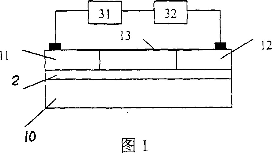
[0029] The fabrication of the photoelectric sensor of the present invention generally includes: MEMS process and one-dimensional semiconductor nanostructure assembly process. The MEMS process is mainly to form a pair of comb electrodes on a single crystal silicon substrate; the assembly of one-dimensional semiconductor nanostructures is mainly to assemble the one-dimensional semiconductor nanostructures on the prepared electrode pairs by electrophoresis. After the above two steps, the photoelectric sensor will be obtained.

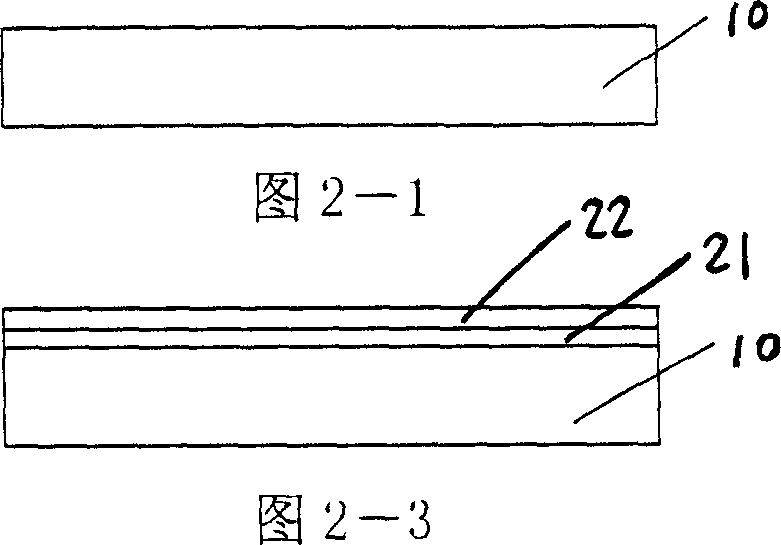
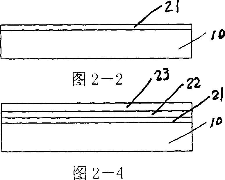
[0030] In one embodiment of the present invention, the photoelectric sensor based on the one-dimensional semiconductor nanostructure after the process of MEMS process and electrophoretic assembly of the one-dimensional semiconductor nanostructure is as shown in Figure 1; Figure 2-1, Figure 2-2, Figure 2-3, Figure...


PUM


Abstract

The invention relates to a photoelectric sensor based on one-dimensional semi-conductor nanometer structure and relative preparation method, which comprises, a single-crystal silicone base; the silicon oxide layer via hot oxygenation method formed by on the surface of single-crystal silicon base and a silicon nitride layer via the low-pressure chemical vapor deposition or plasma strengthen chemical vapor deposition deposited on the surface of silicon oxide layer. Wherein, the silicon oxide layer and the silicon nitride layer can form an insulation layer. And the invention also comprises the comb electrode couple formed by the first comb electrode and the second comb electrode prepared on the surface of insulation layer via the photo-etching / ion-etching method; the multi-tooth end of said electrode couple are oppositely arranged between which a one-dimensional semi-conductor nanometer structure is arranged. The invention has the advantages that: the preparation of micro electrode couple is standard micro processing technology which is simple; the one-dimensional semi-conductor nanometer structure is small, with large surface / volume rate and high photoelectric efficiency, while using simple electrophoresis integration to realize batch production. Said photoelectric sensor has small size, high sensitivity and the application for photo detection and light switch.

Description

technical field [0001] The invention relates to the field of photoelectric sensors, in particular to a photoelectric sensor based on a one-dimensional semiconductor nanostructure and a manufacturing method thereof. Background technique [0002] Photoelectric sensors are key components in modern information detection technology. How to improve the photosensitivity of photosensitive sensing structures and improve the performance of photosensitive units has become a major research problem in this field. Under illumination, the semiconductor photosensitive structure will absorb the incident light. After the incident light is absorbed in the light-sensitive structure, it is excited to generate photo-generated carriers, which leads to a change in resistance. By measuring the change in resistance of the light-sensitive structure, the change in light intensity can be obtained. [0003] The sensitivity of the photoelectric sensor is directly related to the surface area / volume ratio...

Claims


Application Information

Patent Timeline
Patent Type & Authority Applications(China)
IPC IPC(8): H01L31/09H01L31/18
CPCY02P70/50
Inventor 周兆英朱荣王鼎渠叶雄英
Owner TSINGHUA UNIV
Why Eureka
Try Eureka