
Double gate memory cell with improved tunnel oxide

A technology of memory cell and tunnel oxide layer, which is applied in the direction of electrical components, transistors, electric solid-state devices, etc., to achieve the effect of increasing the Fermi energy level difference and reducing the barrier height

Inactive Publication Date: 2006-08-02
INFINEON TECH AG
View PDF0 Cites 2 Cited by
  • Summary
  • Abstract
  • Description
  • Claims
  • Application Information

AI Technical Summary

Problems solved by technology

For this reason, there are currently no conclusive proposals on how NOR and NAND memory cells with minimum feature sizes smaller than 80nm can be scaled without interference

Method used


Image

  • Double gate memory cell with improved tunnel oxide
  • Double gate memory cell with improved tunnel oxide
  • Double gate memory cell with improved tunnel oxide

Examples


Embodiment Construction

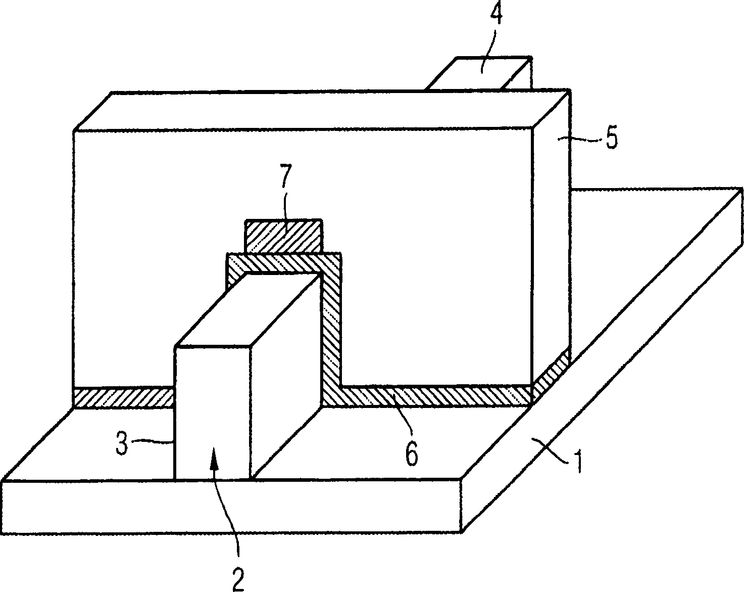
[0023] schematically showing a perspective view of a conventional FinFET transistor structure figure 1 This has already been explained at the beginning, so further description can be omitted here.

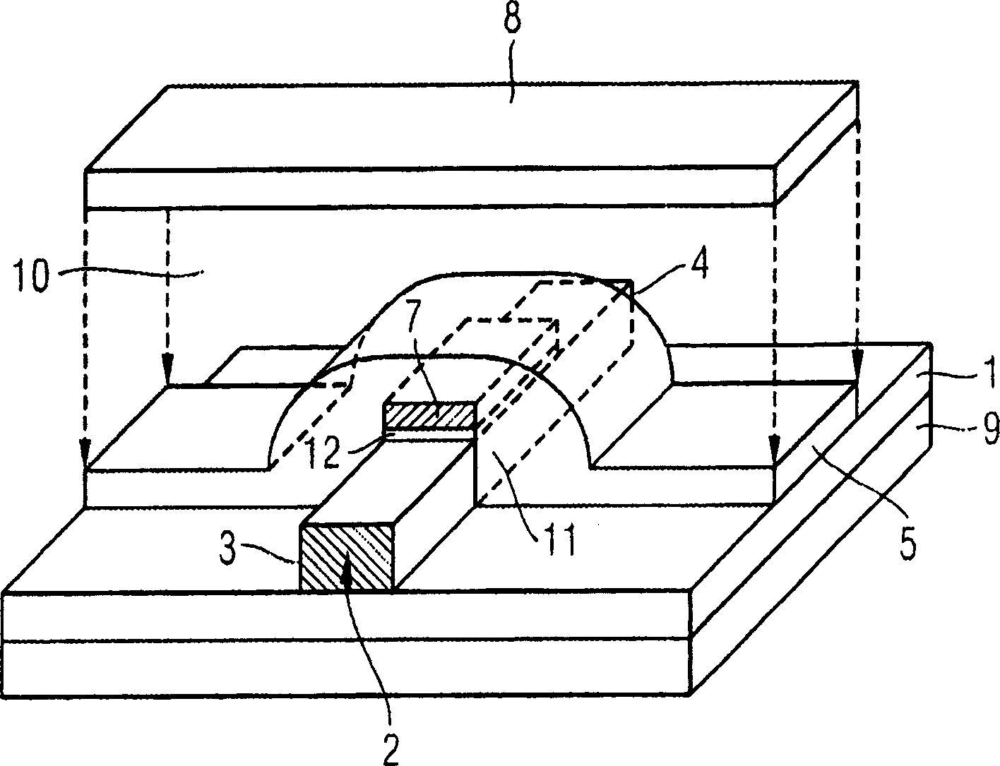
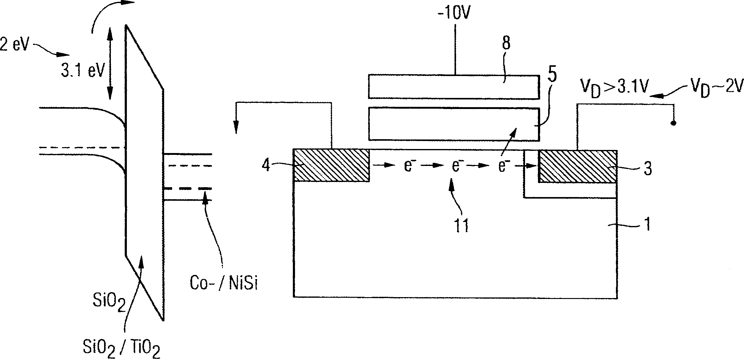
[0024] exist figure 2 The dual-gate memory cell of the present invention is schematically illustrated in . Thus, on the n-type silicon substrate 1 supported by the insulating material 9 ridged wings 2 are formed, within which ridged wings constitute the active region. The active region includes a drain region 3 and a source region 4, and a channel region 11 therebetween. The channel region 11 is surrounded by the floating gate 5 on the side parallel to the substrate surface and on both sides perpendicular to the substrate surface. A tunnel oxide layer 7 is formed between the floating gate 5 and the channel region 11 on the side parallel to the substrate surface, and electrons can tunnel through the tunnel oxide layer 7 to charge or discharge the floating gate 5 . An insulating...


PUM


Abstract

Provides a double gate memory cell having a silicon substrate with an active region having a channel region and source / drain regions, the active region forming a ridgelike fin with at least the channel region. A tunnel oxide layer is formed at least partly on the surface of the ridgelike fin of the active region. A floating gate for storing electrical charges is formed at least partly on the surface of the tunnel oxide layer. An intergate insulator layer made of a dielectric material is formed at least partly on the surface of the floating gate. A control gate is formed at least partly on the surface of the intergate layer, the tunnel oxide layer including an amorphous silicon dioxide / titanium dioxide mixed oxide.

Description

technical field [0001] The present invention is in the technical field of semiconductor devices, and in particular relates to double-gate memory cells, as typically used in flash memory. Background technique [0002] First, considering modern portable devices such as MP3 players and digital video cameras, the demand for inexpensive, high-density and high-capacity memory has greatly increased in recent years. In order to increase storage density, it is necessary to reduce the memory cell size, however this brings a series of problems such as, for example, structural impreciseness and narrow processing window. In particular, parasitic coupling currents rise during scaling, which creates problems mainly in the case of adjacent floating gates in NAND type memory cell devices. Furthermore, shrinking the tunnel oxide is intractable in view of the programming and data retention characteristics of the memory cell, since the undesired short channel effect becomes greater with shrink...

Claims


Application Information

Patent Timeline
Patent Type & Authority Applications(China)
IPC IPC(8): H01L29/788H01L29/51H01L27/115H10B41/00H10B41/27H10B41/35H10B69/00
CPCH01L29/7881H01L29/785H01L29/66825H01L21/28273H01L29/40114H10B41/35
Inventor K·-D·乌费尔特
Owner INFINEON TECH AG
Learn More