Method for preparing poly crystal germanium silicon film

A technology of silicon thin film and polycrystalline germanium, which is applied in the field of preparation of polycrystalline silicon germanium thin film, can solve the problems of poor crystal quality, low carrier mobility, and many defects

Inactive Publication Date: 2006-08-23
ZHEJIANG UNIV
View PDF0 Cites 0 Cited by
  • Summary
  • Abstract
  • Description
  • Claims
  • Application Information

AI Technical Summary

Problems solved by technology

[0002] The growth of polycrystalline silicon germanium thin films by chemical vapor deposition has the characteristics of uniform deposition of silicon germanium thin films and high growth efficiency. However, at present, chemical vapor deposition methods are used to grow polycrystalline silicon germanium thin films, and most of them are grown by constant pressure methods. Due to the high growth pressure, As a result, nucleation and growth are alternately carried out during the preparation of thin films, the crystallization is not uniform enough, the crystal quality is poor, there are many defects, and the carrier mobility is not high

Method used


Image

  • Method for preparing poly crystal germanium silicon film

Examples


Embodiment 1

[0014] 1) Clean the silicon substrate and put it into a thermal oxidation furnace, feed oxygen with a purity of 99.99%, and thermally oxidize a layer of 0.2 μm silicon dioxide at 1000°C;

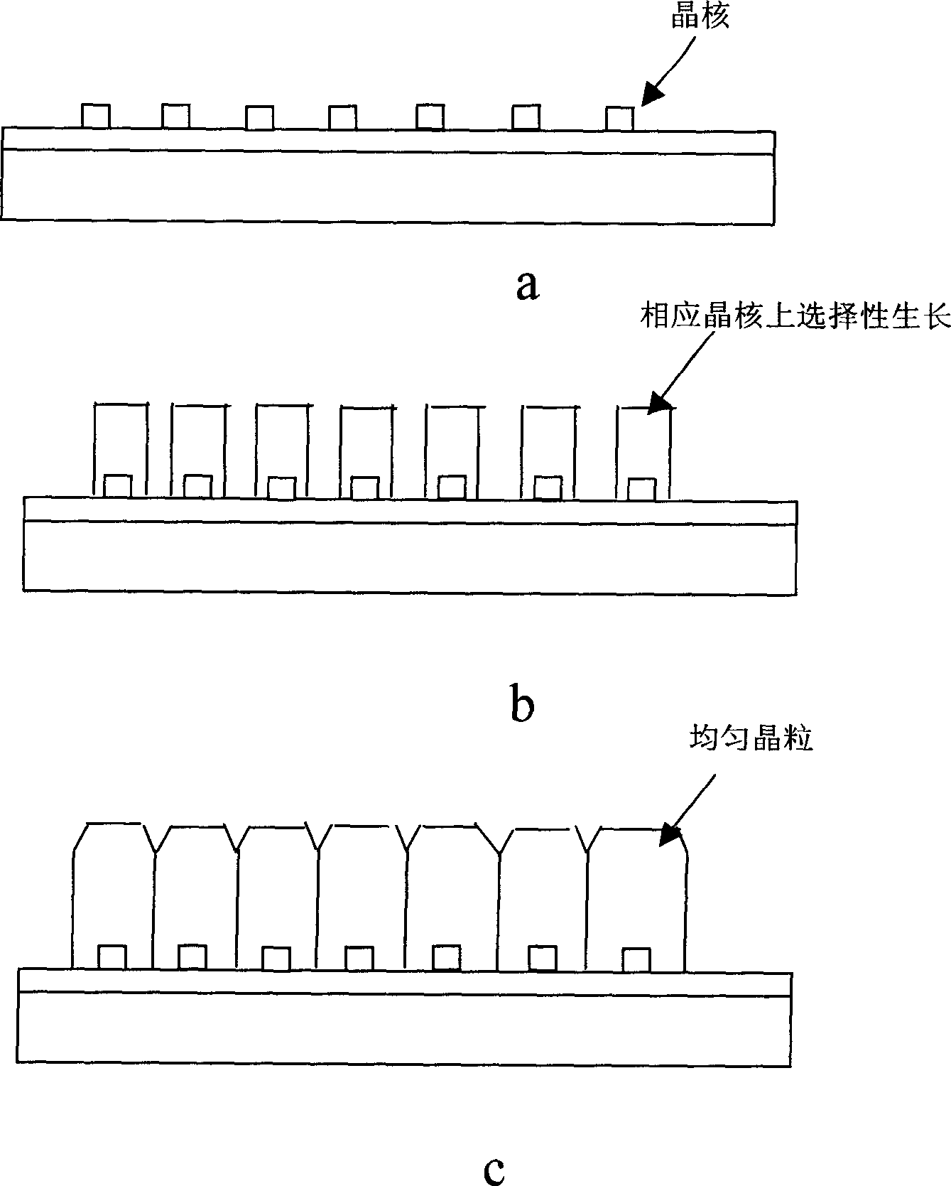
[0015] 2) Put the sample into an ultra-high vacuum chemical vapor deposition system, and at 550°C, feed silane with a purity of 99.999% and a mixed gas of germane and hydrogen with a germane content of 10%, and control the flow of the silane and mixed gas The ratio is 5:5, the pressure in the growth chamber is 10Pa, and the growth takes 15 minutes to form silicon germanium crystal nuclei on the surface of silicon dioxide, as shown in Figure 1a;

[0016] 3) Reduce the growth pressure in the growth chamber to 0.01Pa, keep the temperature at 550°C and the flow ratio of silane and mixed gas at 5:5, and selectively grow at the SiGe crystal nucleus (see Figure 1b) for 20 minutes Finally, a polycrystalline silicon germanium thin film with uniform crystal quality in the growth direction is obtained....

Embodiment 2

[0018] 1) Clean the silicon substrate and put it into a thermal oxidation furnace, feed oxygen with a purity of 99.99%, and thermally oxidize a layer of 0.3 μm silicon dioxide at 1000°C;

[0019] 2) Put the sample into an ultra-high vacuum chemical vapor deposition system, and at 600°C, feed disilane with a purity of 99.999% and a mixed gas of germane and hydrogen with a germane content of 10%, and control the disilane and mixed gas The flow rate ratio is 5:5, the pressure in the growth chamber is 20Pa, and the growth time is 10 minutes, forming silicon germanium crystal nuclei on the surface of silicon dioxide;

[0020] 3) Reduce the growth pressure in the growth chamber to 0.1Pa, keep the temperature at 600°C and the flow ratio of disilane and mixed gas at 5:5, and selectively grow at the silicon germanium nucleus. After 30 minutes of growth, the obtained Polycrystalline silicon germanium film with uniform crystal quality in the growth direction.


PUM


Abstract

Present invention discloses polycrystalline germanium silicon thin-film preparation method. It contains washing up silicon substrate then putting in thermal oxidizer, thermooxidizing single-layer silicon dioxide on silicon substrate, then putting sample in ultrahigh vacuum chemical vapour plating device, at 500-600 degree centigrade filling in pure silicon source and germane using hydrogen as carrier gas, controlling growth room pressure at 10-20 Pa to form germanium silicon crystal nucleus on silicon dioxide surface, reducing grown pressure to 0.01-0.1 Pa and keeping growth parameter unchanged, selective growth on germanium silicon crystal nucleus to form continuous film. Said invention can obtain crystal mass homogeneous polycrystalline germanium silicon film in film growth direction.

Description

technical field [0001] The invention relates to the preparation of semiconductor materials, in particular to the preparation method of polycrystalline germanium silicon thin film. Background technique [0002] The growth of polycrystalline silicon germanium thin films by chemical vapor deposition has the characteristics of uniform deposition of silicon germanium thin films and high growth efficiency. However, at present, chemical vapor deposition methods are used to grow polycrystalline silicon germanium thin films, and most of them are grown by constant pressure methods. Due to the high growth pressure, As a result, nucleation and growth are alternately carried out during the preparation of thin films, the crystallization is not uniform enough, the crystal quality is poor, there are many defects, and the carrier mobility is not high. Contents of the invention [0003] The object of the present invention is to provide a method for preparing a polycrystalline silicon german...

Claims


Application Information

Patent Timeline
Patent Type & Authority Applications(China)
IPC IPC(8): H01L21/205C23C16/52
Inventor 叶志镇吴贵斌赵星刘国军赵炳辉
Owner ZHEJIANG UNIV
Why Eureka
Try Eureka