Inductance coupled coil and inductance coupled plasma device

A technology of inductively coupled coils and coils, applied in the direction of plasma, coils, circuits, etc., can solve the problems of increased volume, uneven etching rate, difficult plasma density, etc., to improve quality, improve distribution uniformity, improve The effect of uniformity

Active Publication Date: 2006-08-30
BEIJING NAURA MICROELECTRONICS EQUIP CO LTD
View PDF0 Cites 11 Cited by
  • Summary
  • Abstract
  • Description
  • Claims
  • Application Information

AI Technical Summary

Problems solved by technology

The volume of the reaction chamber 4 also increases accordingly. It is very difficult to achieve a uniform plasma density by diffusion. Therefore, most of the current etching equipment has the problem of uneven etching rate, which has a great impact on the semiconductor manufacturing process. had a great adverse effect on

Method used


Image

  • Inductance coupled coil and inductance coupled plasma device
  • Inductance coupled coil and inductance coupled plasma device
  • Inductance coupled coil and inductance coupled plasma device

Examples


Embodiment 1

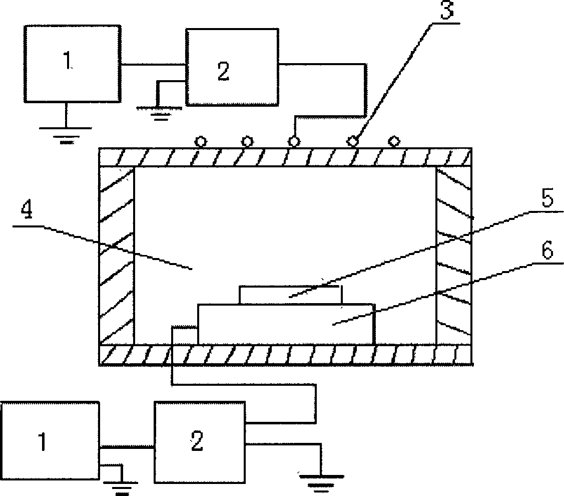
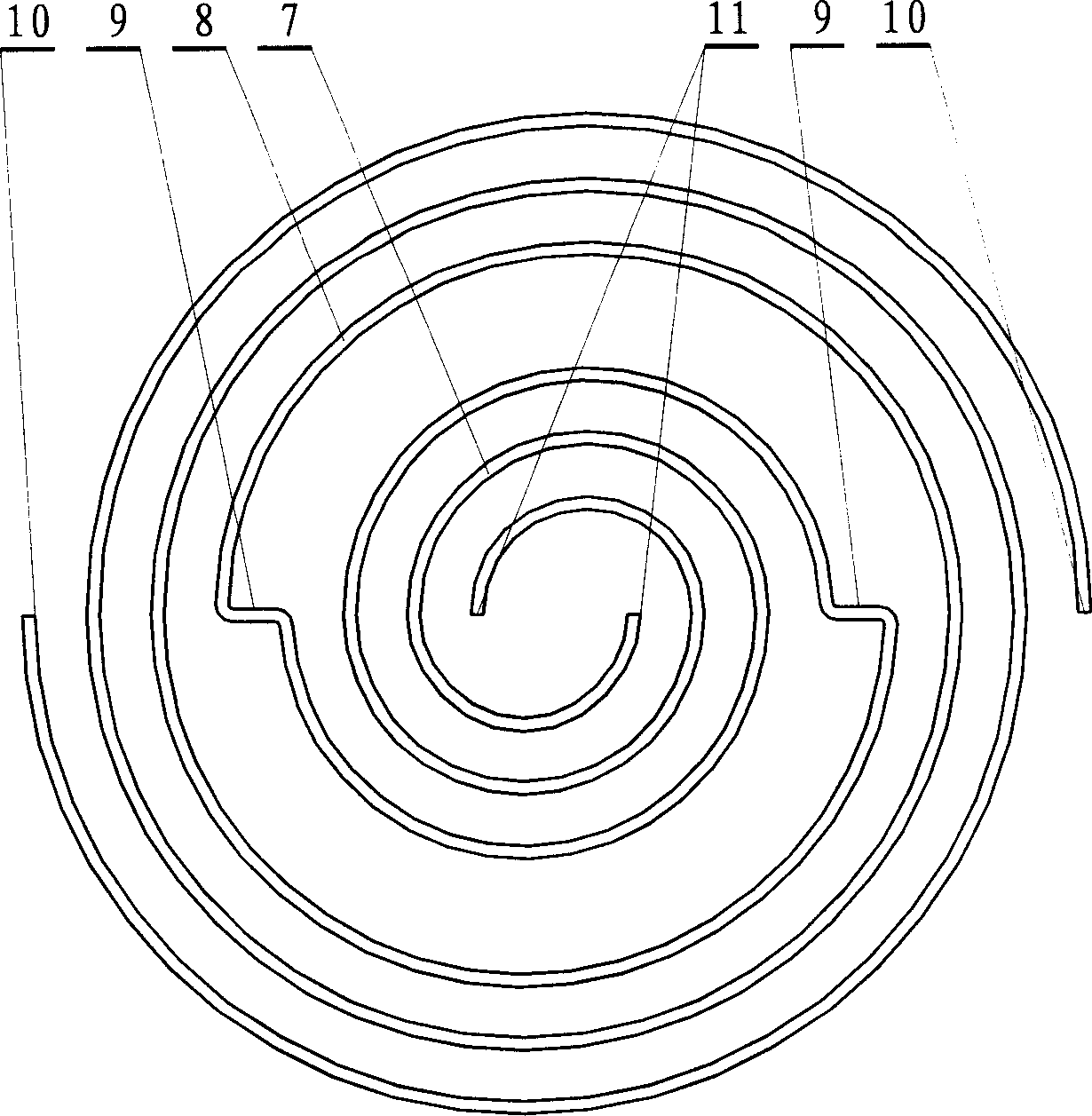
[0027] For a wafer 5 of 300mm, use such as image 3 In the shown inductive coupling coil, a set of involute coils of the inductive coupling coil is composed of an inner coil 7 and an outer coil 8, the inner coil 7 is a one-and-a-half-turn involute-shaped coil, and the outer coil 8 is a one-and-a-half turn involute coil Wire-shaped coils; the inner coil 7 and the outer coil 8 are connected in series through a connecting coil 9 to form a group of involute coils. Two sets of involute coils are nested to form an inductively coupled coil. The two ends of the inner ring of the two sets of involute coils are the output ends 11 , and the two ends of the outer ring are the input ends 10 . Of course, according to different requirements in practical applications, the inner coil 7 and the outer coil 8 may also adopt involute coils with less than one and a half turns or more.

Embodiment 2

[0029] Such as Figure 4 As shown, a group of involute coils of an inductively coupled coil is composed of an inner coil 7 and an outer coil 8, the inner coil 7 is a two-turn involute-shaped coil, and the outer coil 8 is a two-turn involute-shaped coil; The coil 7 and the outer coil 8 are connected in series through a connecting coil 9 to form a group of involute coils. Two sets of involute coils are nested to form an inductively coupled coil. The two ends of the inner circle of the two groups of involute coils are input ends 10 , and the two ends of the outer circle are output ends 11 .

Embodiment 3

[0031] For a 200mm wafer 5, such as Figure 5 In the shown inductive coupling coil, a group of involute coils of the inductive coupling coil is a two-and-a-half-turn involute-shaped coil, and two sets of involute coils are nested to form the inductive coupling coil. The two ends of the inner ring of the two sets of involute coils are the output ends 11 , and the two ends of the outer ring are the input ends 10 . Certainly, according to different requirements in practical applications, the involute coil may be an involute-shaped coil with less than two and a half turns or more.


PUM


Abstract

The invention is an inductance coupling coil, nested of two groups of involute coils, where the involute coil can be a segment of involute, or composed of inner and outer coils of an involute shape, and the two groups of involute coils are the same in shape and centro-symmetrically distributed. And the design of a completely symmetrical plane coil structure makes electromagnetic field distribution in a reaction chamber quite symmetrical, thus improving distribution uniformity of plasma in the reaction chamber so as to make etching rates of all points on the surface of a wafer closer. And an inductance coupled plasma device of this structure reduces the inductance of the inductance coupling coil, thus able to be very easy to obtain a large-area plasma and improve plasma uniformity in the large-area process. And it can improve the quality of etching wafer.

Description

technical field [0001] The invention relates to an accessory for semiconductor wafer processing equipment, in particular to an inductively coupled coil and an inductively coupled plasma device. Background technique [0002] At present, with the rapid development of electronic technology, people have higher and higher requirements for the integration of integrated circuits, which requires enterprises that produce integrated circuits to continuously improve the processing capacity of semiconductor wafers. Plasma devices are widely used in fabrication processes for fabricating integrated circuits (ICs) or MEMS devices. Among them, inductively coupled plasma (ICP) is widely used in etching and other processes. Under low pressure, the reactive gas is excited by radio frequency power to generate ionization to form a plasma. The plasma contains a large number of active particles such as electrons, ions, excited atoms, molecules and free radicals. These active reactive groups and t...

Claims


Application Information

Patent Timeline
Patent Type & Authority Applications(China)
IPC IPC(8): H01F5/00H01L21/3065H05H1/34H05H1/00
Inventor 宋巧丽李东三孙岩
Owner BEIJING NAURA MICROELECTRONICS EQUIP CO LTD
Why Eureka
Try Eureka