Method for making double layer grid dielectric layer

A dielectric layer and double-layer gate technology, which is applied in the manufacture of circuits, electrical components, semiconductors/solid-state devices, etc.

Inactive Publication Date: 2006-08-30
UNITED MICROELECTRONICS CORP
View PDF0 Cites 6 Cited by
  • Summary
  • Abstract
  • Description
  • Claims
  • Application Information

AI Technical Summary

Problems solved by technology

[0006] Therefore, the main purpose of the present invention is to provide a method for making a double-layer gate dielectric layer, so as to overcome the unsolvable problems in the prior art

Method used


Image

  • Method for making double layer grid dielectric layer
  • Method for making double layer grid dielectric layer
  • Method for making double layer grid dielectric layer

Examples


Embodiment Construction

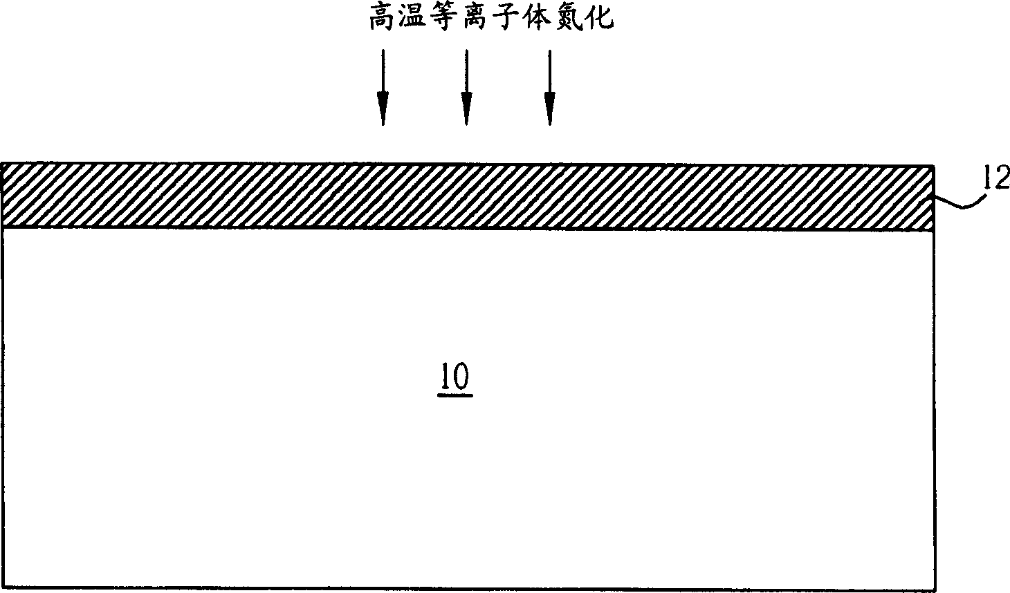
[0019] Please refer to Figure 5 to Figure 10 . Figure 5 to Figure 10 A schematic diagram of a method for fabricating a double-layer gate dielectric layer according to a preferred embodiment of the present invention. Such as Figure 5 As shown, first a semiconductor substrate 50 is provided, such as a silicon substrate, and a silicon dioxide film 52 is formed on the surface of the semiconductor substrate 50, wherein in this embodiment, the silicon dioxide film 52 utilizes a chemical vapor deposition process, and silicon dioxide The thickness of the film is between 5-80 angstrom, and the process temperature of the chemical vapor deposition process is kept below 400° C. to maintain a good interface between the silicon dioxide film 52 and the semiconductor substrate 50 . However, the formation method of the silicon dioxide film 52 is not limited thereto, and the visible effect is formed by other methods, such as a thermal oxidation process.

[0020] Such as Figure 6 As show...


PUM


Abstract

The invention is a method for making a double-layer grid dielectric layer, firstly providing a semiconductor substrate and forming a silicon dioxide film on the semiconductor substrate, successively forming a noncrystalline silicon film on the silicon dioxide film and making a low-temperature plasma nitrogenization process to form the noncrystalline silicon film into a nitrogenous noncrystalline silicon film, and finally making an oxygen gas annealing process to make the oxygen gas react with the nitrogenous noncrystalline silicon film so as to form a nitrogen-enriched silicon oxynitride layer.

Description

technical field [0001] The invention relates to a method for manufacturing a double-layer grid dielectric layer, in particular to a method for manufacturing a double-layer grid dielectric layer composed of a silicon dioxide film and a nitrogen-rich nitrogen oxide silicon layer. Background technique [0002] With the rapid development of semiconductor technology, the line width of the semiconductor process is also continuously reduced. According to the current technology, the gate width has progressed to 70nm, and the thickness of the gate oxide layer has also shrunk to about 1.5nm. As the thickness of the gate oxide layer decreases, the problem of gate leakage current also arises accordingly. Therefore, the current practice of using a silicon oxynitride layer with a high dielectric constant to replace the traditional silicon oxide as the gate dielectric layer, due to the same The equivalent oxide thickness (EOT) has a thicker thickness, which can avoid the generation of gate...

Claims


Application Information

Patent Timeline
Patent Type & Authority Applications(China)
IPC IPC(8): H01L21/314H01L21/28H01L21/336
Inventor 郑博伦程立伟
Owner UNITED MICROELECTRONICS CORP
Why Eureka
Try Eureka