Method of forming a nanogap and method of manufacturing a nano field effect transitor for molecular device and bio-sensor, and molecular device and bio-sensor manufactured using the same

A field-effect transistor and biosensor technology, which is applied in the fields of forming nano-gap, nano-field-effect transistors for molecular devices and biosensors, and molecular devices and biosensors made by the nano-gap, can solve complex procedures, heavy workloads, etc. Problems such as low visibility, light source dispersion phenomenon, etc.

Inactive Publication Date: 2006-09-06
KOREA ADVANCED INST OF SCI & TECH
View PDF0 Cites 15 Cited by
  • Summary
  • Abstract
  • Description
  • Claims
  • Application Information

AI Technical Summary

Problems solved by technology

[0014] However, the formation of gaps with a size smaller than a few nanometers by the photolithography method used in conventional silicon processing has technical limitations, such as the wavelength of the light source used and the dispersion phenomenon of light, etc.
In addition, since the use of photolithography to form the nanogap requires a complicated process and the method becomes less reproducible as the required gap size becomes smaller, the size required to form a high-performance biosensor is several nanometers. clearance is hard

Method used


Image

  • Method of forming a nanogap and method of manufacturing a nano field effect transitor for molecular device and bio-sensor, and molecular device and bio-sensor manufactured using the same
  • Method of forming a nanogap and method of manufacturing a nano field effect transitor for molecular device and bio-sensor, and molecular device and bio-sensor manufactured using the same
  • Method of forming a nanogap and method of manufacturing a nano field effect transitor for molecular device and bio-sensor, and molecular device and bio-sensor manufactured using the same

Examples


Embodiment Construction

[0036] Hereinafter, a method of forming a nanogap for a molecular device or a biosensor and a method of manufacturing a nanofield effect transistor for a molecular device or a biosensor will be described in detail according to preferred embodiments of the present invention with reference to the accompanying drawings.

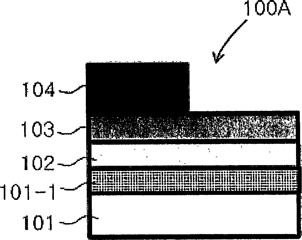
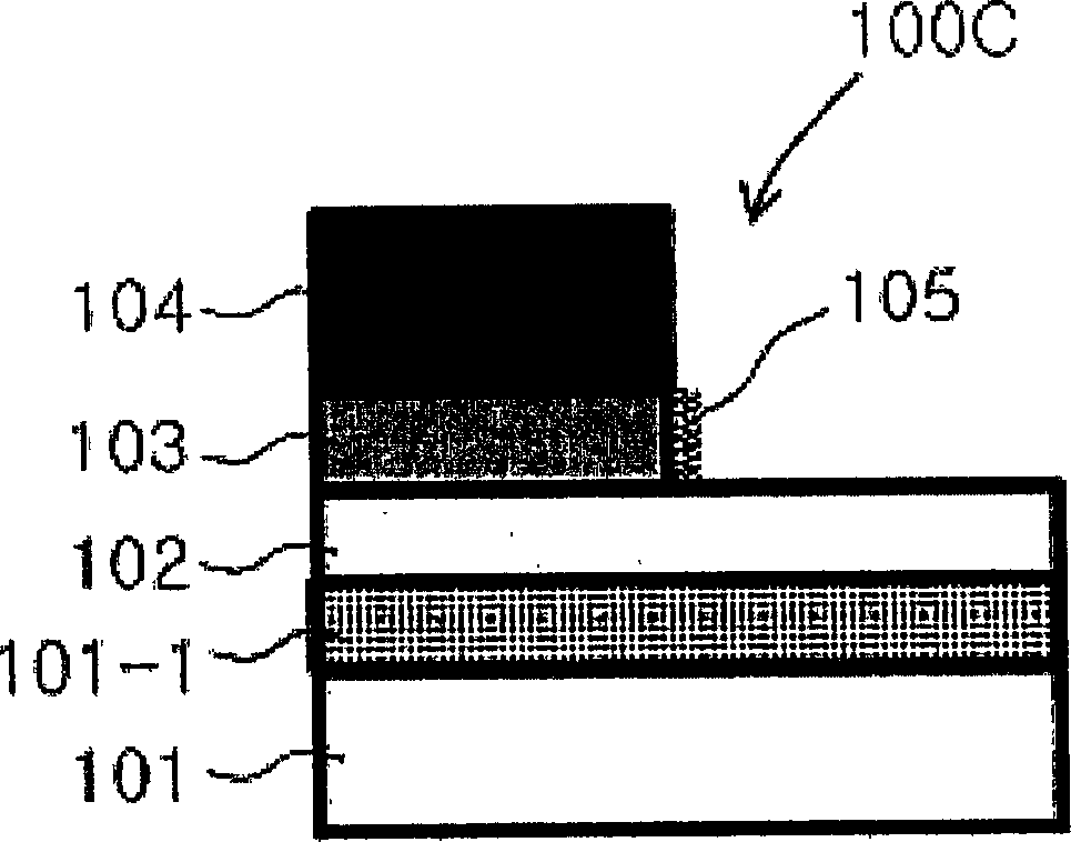
[0037] Figure 1a-1f is a series of cross-sectional views showing sequentially a method of forming a planar nanogap for a biosensor according to an embodiment of the present invention.

[0038] As shown in the figure, a first gold (Au) layer (metal layer) is formed on a silicon substrate, and a second gold layer isolated from the first gold layer is formed using a self-assembled monolayer (hereinafter referred to as "SAM") , thus forming a planar nanogap corresponding to the length of the SAM.

[0039] The method of forming the nanogap is described in detail as follows.

[0040] First, a back gate thin layer 101-1, an insulating layer 102, a first gold layer 10...


PUM


Abstract

The present invention relates to a method of forming a nanogap, a method of manufacturing a nano field effect transistor for a molecular device or a bio-sensor, and a fabrication thereof, and more particularly, to a method of forming a high reproductive nanogap using a thin layer with a molecular size or a size which is similar to that of a molecule and a nano field effect transistor manufactured by the method of forming the nanogap. The method of forming a nanogap according to the present invention comprises steps of (a) forming sequentially an insulating layer, a first metal layer and a hard mask on a silicon substrate; (b) etching partially the first metal layer using the mask as an etching mask; (c) forming a self-assembled monolayer (SAM) on a side surface of the first metal layer to form a nanogap on the silicon substrate; (d) depositing metal on the entire structure including the mask to form a second metal layer; (e) removing the metal deposited on the hard mask using a lift-off process by etching the mask formed in step (a) and (f) etching the SAM formed in step (c) to form the nanogap.

Description

technical field [0001] The present invention relates to methods of forming nanogaps, fabrication methods and structures of nanofield-effect transistors (nanoFETs) for use in molecular devices or biosensors, and more particularly to the use of nanometers with dimensions as thin as or similar to molecular dimensions A method for forming a highly reproducible nano-gap with a thin film, and a nano-field-effect transistor manufactured by the method for forming a nano-gap. Background technique [0002] Metallic nanogap with metal plates on both sides of the nanoscale gap is of great value in the fabrication of molecular devices and biosensors. [0003] As technology continues to develop, high integration of semiconductor devices has been achieved along with high performance and miniaturization. [0004] Device miniaturization is currently reaching its limits due to technical limitations of photolithography (light source wavelength, light dispersion, lens numerical aperture (N / A),...

Claims


Application Information

Patent Timeline
Patent Type & Authority Applications(China)
IPC IPC(8): H01L21/336B82B3/00
CPCB82Y10/00G01N33/54373B82Y15/00G01N2610/00G01N33/552G01N33/553B82Y30/00F16F1/38F16F15/08
Inventor 崔梁圭金洲铉
Owner KOREA ADVANCED INST OF SCI & TECH
Why Eureka
Try Eureka