Method for changing polar of gallium nitride epitaxial layer grown by hydride vapour phase epitaxy method

A hydride vapor phase and epitaxial growth technology, applied in coatings, electrical components, gaseous chemical plating, etc., can solve problems such as reducing the dislocation density of GaN thin films, and achieve the effects of low cost, simple and easy method, and improved performance.

Inactive Publication Date: 2006-09-13
SHANGHAI INST OF MICROSYSTEM & INFORMATION TECH CHINESE ACAD OF SCI
View PDF0 Cites 7 Cited by
  • Summary
  • Abstract
  • Description
  • Claims
  • Application Information

AI Technical Summary

Problems solved by technology

W. Zhang et al. used the method of growth interruption to release the stress of GaN epitaxial growth and reduce the dislocation density of GaN films [W. Zhang et al. Appl. Phys. Lett., V78, 772, 2001], but how to The conversion of polar materials to Ga polarity is rarely reported

Method used


Image

  • Method for changing polar of gallium nitride epitaxial layer grown by hydride vapour phase epitaxy method
  • Method for changing polar of gallium nitride epitaxial layer grown by hydride vapour phase epitaxy method

Examples


Embodiment 1

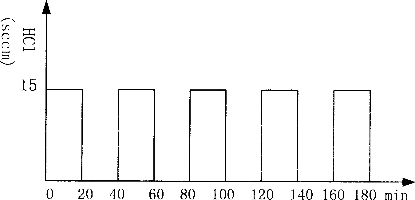
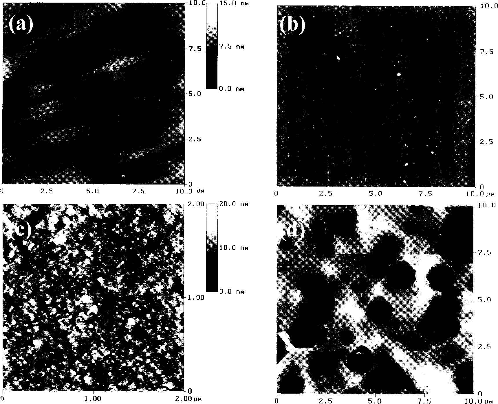
[0016] The method provided by the invention is used in HVPE to change the polarity of GaN material growth, and the growth of GaN adopts Al 2 o 3 As a substrate, first pass NH at high temperature 3 to Al 2 o 3 The substrate was nitrided for 7min, NH 3 The flow rate is 500 sccm, so that the thin AlN island structure is formed on the surface to facilitate the nucleation of GaN. Then grow with HCl gas, at this time the surface of the grown GaN film shows N polarity. After growing for 30min, the thickness of the GaN film was 10μm, then the HCl gas was turned off, and the reaction gas NH 3 and H 2 or N 2 The gas flow rate of the carrier gas remains constant, and the process lasts for 20 minutes. Then continue to open the HCl gas for growth for 20 minutes, then turn off the HCl gas for 20 minutes, and repeat this 4 times. The obtained GaN material will change from N polarity to Ga polarity with smooth surface and stable chemical properties, and its crystal quality will also b...

Embodiment 2

[0020] GaN is grown on a Si substrate, and the HCl growth is interrupted by the method shown in Example 1. The number of interruptions is 8 times, and each time is 10 minutes. The thickness of the grown N-polar GaN film is 20 μm, and the interrupted growth temperature is 950°C. The surface dislocation density of Ga polar GaN material is 1×10 7 / cm 2 . All the other are similar with embodiment 1.

Embodiment 3

[0022] GaAs substrates are used to grow N-polar GaN materials by molecular beam epitaxy growth method. The interrupted growth temperature is 900-1100°C, the number of interrupts is 2-10 times, and the duration of each time is 1-60min. NH 3 The reaction gas flow rate is 500-700sccm, and the carrier gas is N 2 and H 2 of mixed gas. The resulting GaN material has a surface dislocation density of 1×10⁷ / cm 2 , the surface roughness is only 0.527nm (similar to Example 1).


PUM

PropertyMeasurementUnit
thicknessaaaaaaaaaa
surface roughnessaaaaaaaaaa

Abstract

This invention relates to a method for altering the pole of GaN epitaxial layer grown by HVPE characterizing in applying a method of interrupting HCl growth, which first of all penetrates NH3 to nitride the Sapphire under high temperature then penetrates HCl to grow GaN, this time, the GaN film surface shows N pole, then closes HCl after growing for a period of time and continues NH3 for 1-60min, then opens the HCl to grow GaN film continuously and operates like this for 2-10 times, the pole of GaN turns to Ga of a smooth surface from a rough N pole surface and the dislocation density is reduced and the crystal quality is increased.

Description

technical field [0001] The invention relates to a method for changing the polarity of a gallium nitride (GaN) epitaxial layer grown by a hydride vapor phase epitaxy (HVPE) method. The invention aims at improving the quality of epitaxially grown GaN film, and belongs to the technical field of material preparation. technical background [0002] Group III nitride semiconductor optoelectronic material devices are more and more widely used, but the hexagonal group III nitride is a crystal with strong surface polarity. Due to its uniaxial and noncentrosymmetric structure, it exhibits spontaneous polarization and piezoelectric effects [H. Morkoc, Nitride Semiconductors and Devices, Springer, Heidelberg, 1999]. When material epitaxy forms a heterojunction, even in the absence of stress, a large amount of polarization charges will appear at the interface due to the different spontaneous polarization effects on both sides of the interface, which will cause a very strong internal elec...

Claims


Application Information

Patent Timeline
Patent Type & Authority Applications(China)
IPC IPC(8): H01L21/205C23C16/52
Inventor 雷本亮于广辉齐鸣叶好华孟胜李爱珍
Owner SHANGHAI INST OF MICROSYSTEM & INFORMATION TECH CHINESE ACAD OF SCI
Why Eureka
Try Eureka