

Production method for light emitting element
A technology for a light-emitting device and a manufacturing method, which can be applied to chemical instruments and methods, semiconductor/solid-state device manufacturing, crystal growth, etc., and can solve the problems of reducing radiation intensity and easy deterioration.
- Summary
- Abstract
- Description
- Claims
- Application Information
AI Technical Summary
Problems solved by technology
Method used
Image

Examples
Embodiment 3
[0092] Figure 13 It is a schematic diagram showing an example of a specific light-emitting device in Embodiment 3 of the present invention;
[0093] Figure 14A is description Figure 13 A diagram of an example manufacturing process for a light emitting device;
[0094] Figure 14B is to continue Figure 14A The processing steps diagram;
[0095] Figure 14C is to continue Figure 14B The processing steps diagram;
[0096] Figure 15 is a schematic diagram of the corundum crystal structure;
[0097] Figure 16A is a schematic diagram illustrating the operation of the light-emitting device manufacturing method according to Embodiment 3 of the present invention;
[0098] Figure 16B is description Figure 16A A diagram of subsequent operations;
[0099] Figure 16C is description Figure 16B A diagram of subsequent operations;
[0100] Figure 16D is description Figure 16C A diagram of subsequent operations;
[0101] Figure 17 is an example Figures 14A-14...
Embodiment 1
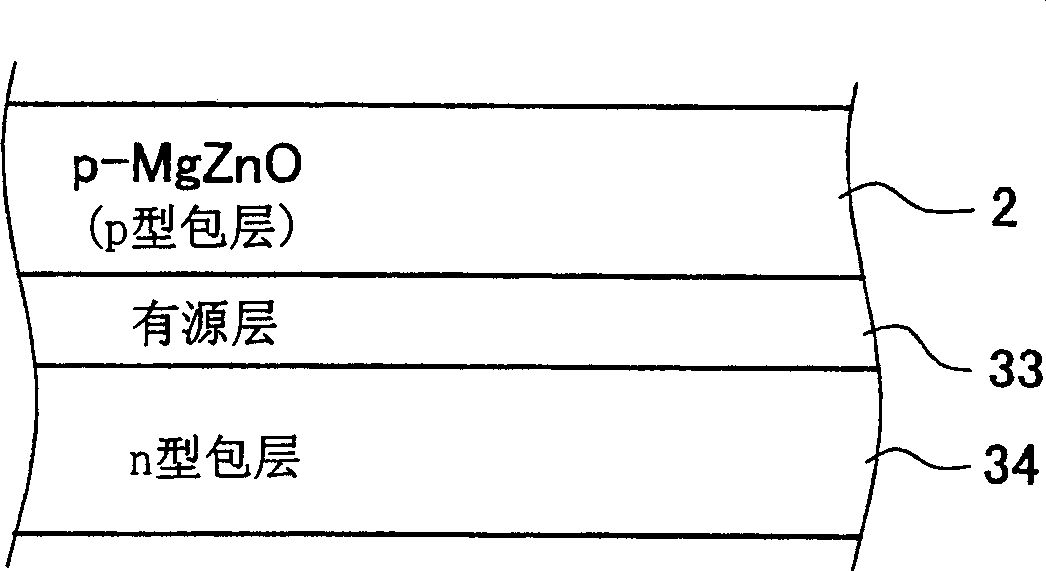
[0114] figure 1 Schematically showing the stacked structure of important parts of the light-emitting device of the first invention, the device has a light-emitting layer portion in which n-type cladding layer 34, active layer 33 and p-type cladding layer 2 are stacked in sequence. The p-type cladding layer 2 is composed of p-type Mg x Zn 1-x O layer (O≤x≤1): hereinafter sometimes referred to as a p-type MgZnO layer 2). In the p-type MgZnO layer 2, one, two or more of trace amounts of N, Ga, Al, In and Li are included as p-type dopants: as mentioned above, the p-type carrier concentration is adjusted in 1×10 16 ~8×10 18 place / cm 3 range, especially at 10 17 ~10 18 place / cm 3 within the range of left and right.
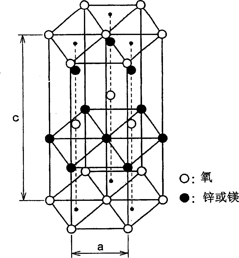
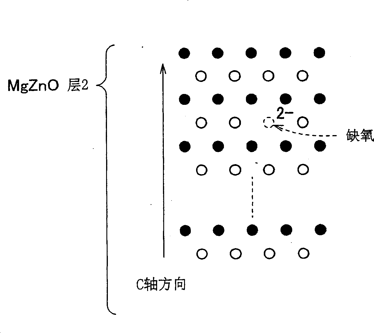
[0115] figure 2 is a schematic diagram of the crystal structure of MgZnO, showing the so-called Wurtzite structure. In this structure, the planes filled with oxygen ions and the planes filled with metal ions (Zn or Mg ions) are alternately stacked along the...
Embodiment 2
[0164] Embodiments of the second invention are described below. Because the basic part of the light-emitting device applicable to the second invention is the same as that described in Embodiment 1, it will not be described in detail (see Figure 1~4 with Figure 10A and 10B ). Such as Image 6 As shown in (a), the GaN buffer layer 11 is epitaxially grown on the sapphire substrate 10, and then a p-type MgZnO layer 52 (generally 50 nm in thickness), an MgZnO active layer 53 (generally 30 nm in thickness) and n Type MgZnO layer 54 (generally 50nm in thickness) (it is also possible to grow in reverse). The epitaxial growth of each layer in this example can be performed by a MOVPE process similar to that described in Example 1, but with the following points of difference. More specifically, when growing the MgZnO active layer 53 and the p-type MgZnO layer 52, an ultraviolet lamp (such as an excimer ultraviolet lamp) as an ultraviolet light source is arranged on the main surfac...
PUM
 Abstract
Description
Claims
Application Information