Grate etching method

An over-etching and gas technology, applied in the field of gate etching, can solve the problems of large gas flow, difficulty in forming a uniform gas flow distribution, poor gas fluidity, etc., and achieve the effect of improving gas flow uniformity, reducing consumption costs and avoiding variables.

Active Publication Date: 2006-10-18
BEIJING NAURA MICROELECTRONICS EQUIP CO LTD
View PDF1 Cites 0 Cited by
  • Summary
  • Abstract
  • Description
  • Claims
  • Application Information

AI Technical Summary

Problems solved by technology

From the above description of the main steps of the etching process, it can be found that the main etching step, which is an important step in the etching process, has a large overall gas flow rate, and at the same time, the mixed gas is mainly composed of large molecular weight Cl. 2 Composed of HBr and HBr, the overall gas fluidity is poor, especially when performing a 300mm silicon wafer etching process, due to the increase in the size of the silicon wafer, it becomes more difficult to form a uniform gas flow distribution on the surface of the silicon wafer

Method used


Image

  • Grate etching method
  • Grate etching method

Examples


Embodiment 1

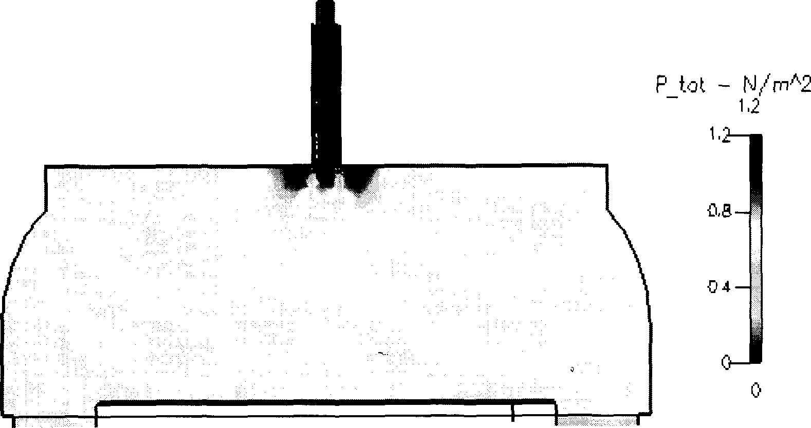
[0026] In the 300mm etching chamber, 20sccm Cl is injected in the main etching step 2 , 250sccmHBr, 10sccmO 2 , 80sccm He, 100sccm N 2 The composition of mixed gas a, gas simulation distribution state see figure 1 .

[0027] The silicon etching equipment used is the North Microelectronics 300mm principle machine, which adopts a single-zone nozzle design, and the nozzle angle is 100-150 degrees.

[0028] The silicon wafer structure used is: silicon wafer = "silicon dioxide (10-100 angstroms) = "polysilicon (1700-2500 angstroms) = "silicon dioxide (100-150 angstroms) = "silicon oxynitride (200-300A ). (The etching pattern has been transferred from the photoresist to the hard mask, that is, the silicon dioxide / silicon oxynitride double layer structure)

[0029] In the etching process, the silicon wafer is first introduced into the etching reaction chamber, and is fixed by the electrostatic chuck. The temperature of the chamber is controlled at 60 degrees Celsius, and the sil...

Embodiment 2

[0035] According to the method described in Example 1, the difference is that, in the main step, pass through 50sccm Cl 2 , 230sccm HBr, 15sccm O 2 , and 150sccm He on the mixed gas, the power of the RF power supply is 400-500W, and the process time is 80-105s.

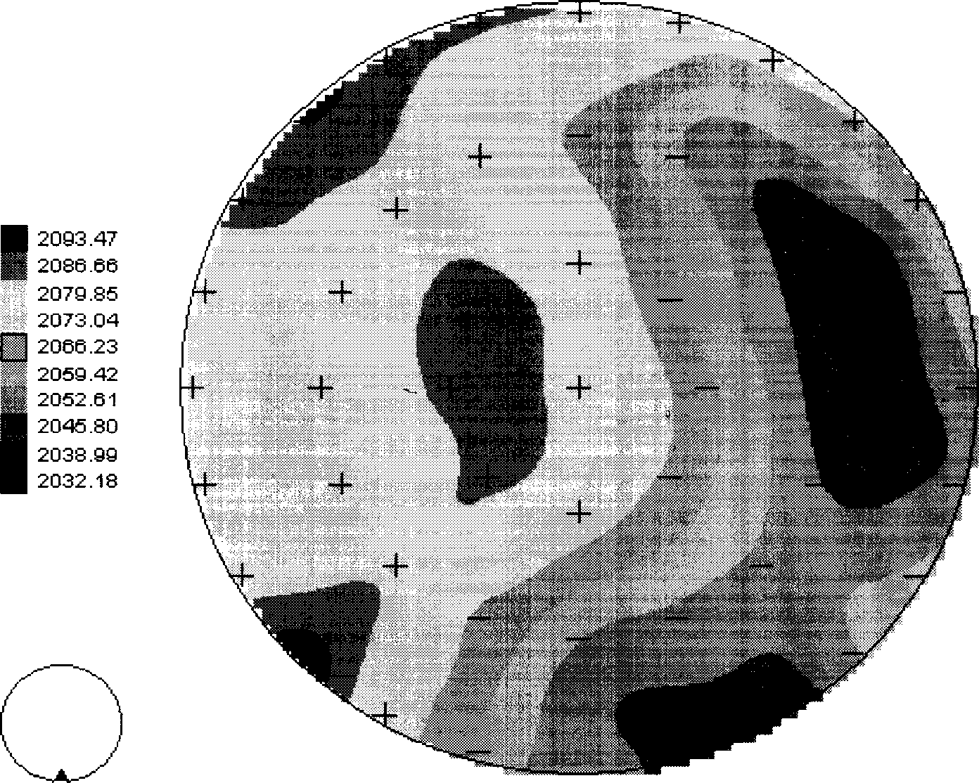
[0036] In the main step gas simulation, the gas flow uniformity on the surface of the silicon wafer is very high, which is 0.5-0.6 Pa. However, because the He gas plasma ignition ability is relatively weak and the plasma concentration is medium, in the actual process, the power of the upper RF power supply is 400 ~500W, the process time is longer, 80~105s. In the final etching result, the etching uniformity of the silicon wafer is as high as 1.80-2.10 (3 Sigma), which can fully meet the needs of the 300mm advanced etching process even without the use of hardware configurations such as dual-zone nozzles to improve the uniformity of the gas flow.

Embodiment 3

[0038] According to the method described in Example 1, the difference is that, in the main step, pass through 50sccm Cl 2 , 230sccm HBr, 15sccm O 2 、150sccmN 2 Composed of gas mixtures. The power of the upper RF power supply is 300-350W, and the process time is 45-65s.

[0039] The gas simulation of the main step, the uniformity of the gas flow on the surface of the silicon wafer is 0.6-0.8Pa, which is better. N2 gas plasma has strong ignition ability and high plasma concentration. Therefore, in the actual process, the power of the upper RF power supply is only 300-350W to maintain the normal etching process, and the process time is very short, 50-65s. The final etching result shows that the etching uniformity of silicon wafers is 2.65-2.90 (3 Sigma), which can basically meet the needs of 300mm advanced etching process when hardware configurations such as dual-zone nozzles are not used to improve airflow uniformity.


PUM

PropertyMeasurementUnit
thicknessaaaaaaaaaa

Abstract

The present invention relates to a gate etching method, including BT step, main etching step and over etching step. It is characterized by that in the described main etching step the used gas contains Cl2, HBr and O2, On the premise of that its hardware design is not changed said method only can change the gas type and matching ratio of main etching step in gate etching process to raise gas flow uniformity of silicon wafer surface process gas so as to meet the requirements of advanced gate etching process.

Description

technical field [0001] The invention relates to a gate etching method, in particular to a method for satisfying the advanced gate etching process by changing the gas type and ratio in the gate etching process. Background technique [0002] As we all know, gaseous plasma technology is widely used in the field of integrated circuit manufacturing, especially in the fields of etching of thin films such as gates, deposition of dielectric materials, and removal of photoresist materials. However, despite the wide acceptance of plasma technology in the semiconductor manufacturing industry, the application of this technology continues to face a considerable number of challenges. It is worth pointing out that a large amount of production / R&D data shows that it is very difficult to ensure that the process gas is evenly distributed on the surface of the semiconductor silicon wafer during the manufacturing process, while the uniform gas flow distribution on the surface of the silicon waf...

Claims


Application Information

Patent Timeline
Patent Type & Authority Applications(China)
IPC IPC(8): H01L21/3065C23F4/00
Inventor 杨柏
Owner BEIJING NAURA MICROELECTRONICS EQUIP CO LTD
Why Eureka
Try Eureka