Fabrication method

A technology of imprinting and liquid layer, applied in the field of forming conductive structures in substrates, can solve problems such as difficulty in arranging resists

Inactive Publication Date: 2006-11-08
INT BUSINESS MASCH CORP
View PDF0 Cites 7 Cited by
  • Summary
  • Abstract
  • Description
  • Claims
  • Application Information

AI Technical Summary

Problems solved by technology

[0007] However, it is difficult to completely dispose the resist over a relatively large area to obtain a pattern with satisfactory contrast

Method used


Image

  • Fabrication method
  • Fabrication method
  • Fabrication method

Examples


Embodiment Construction

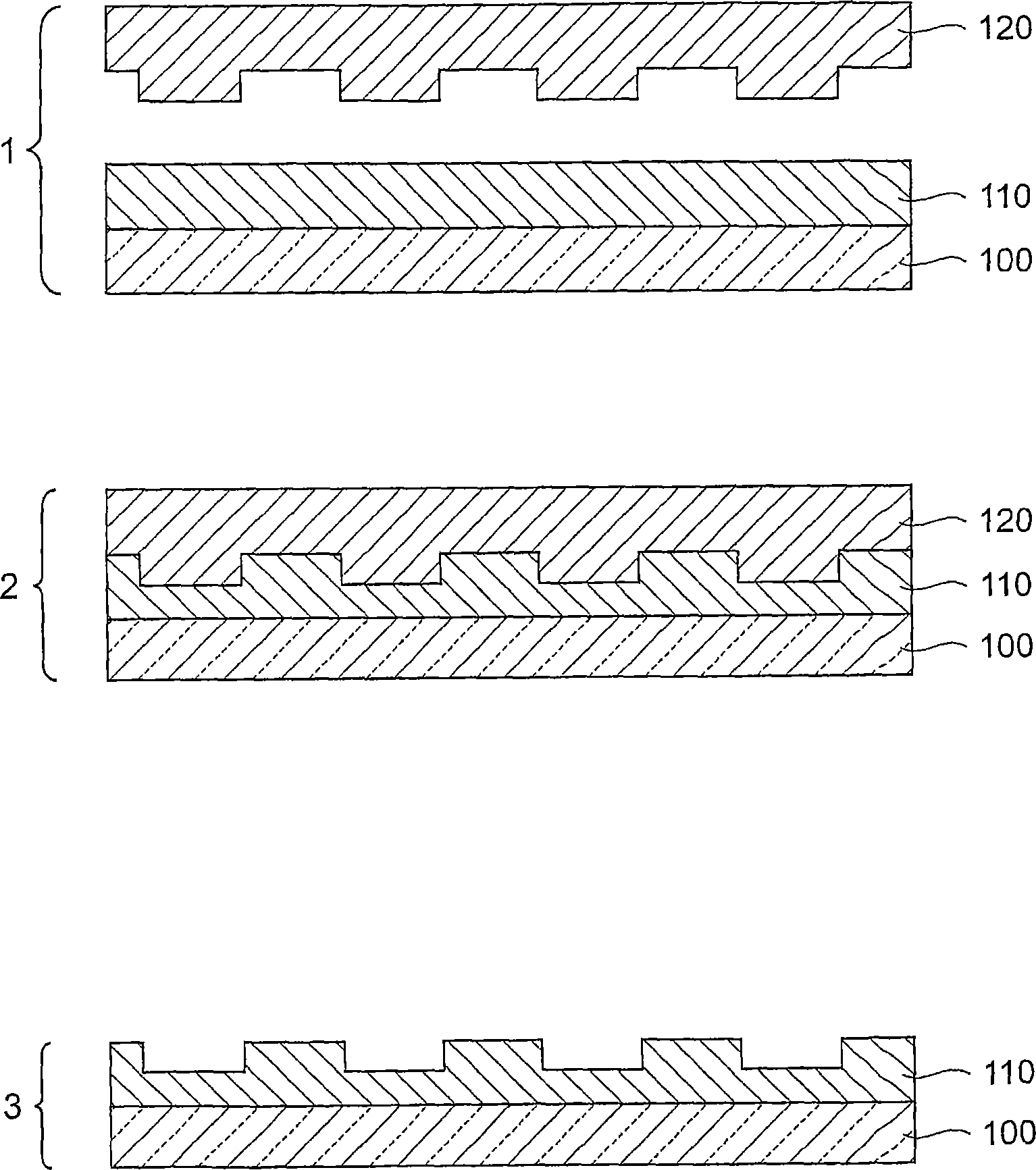
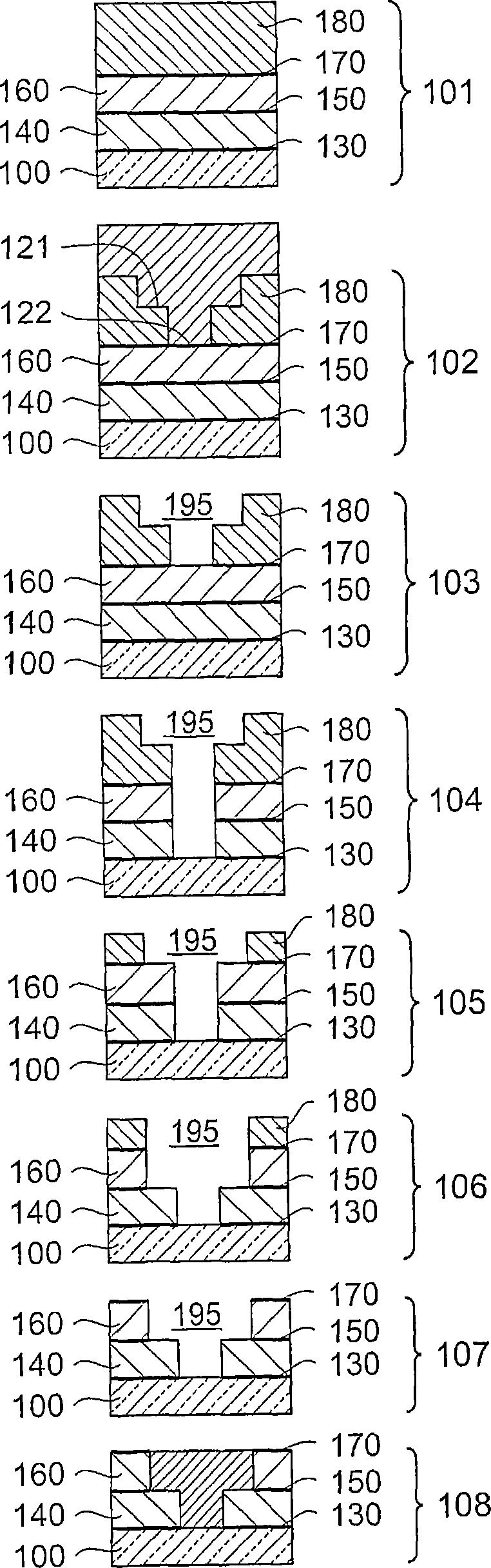
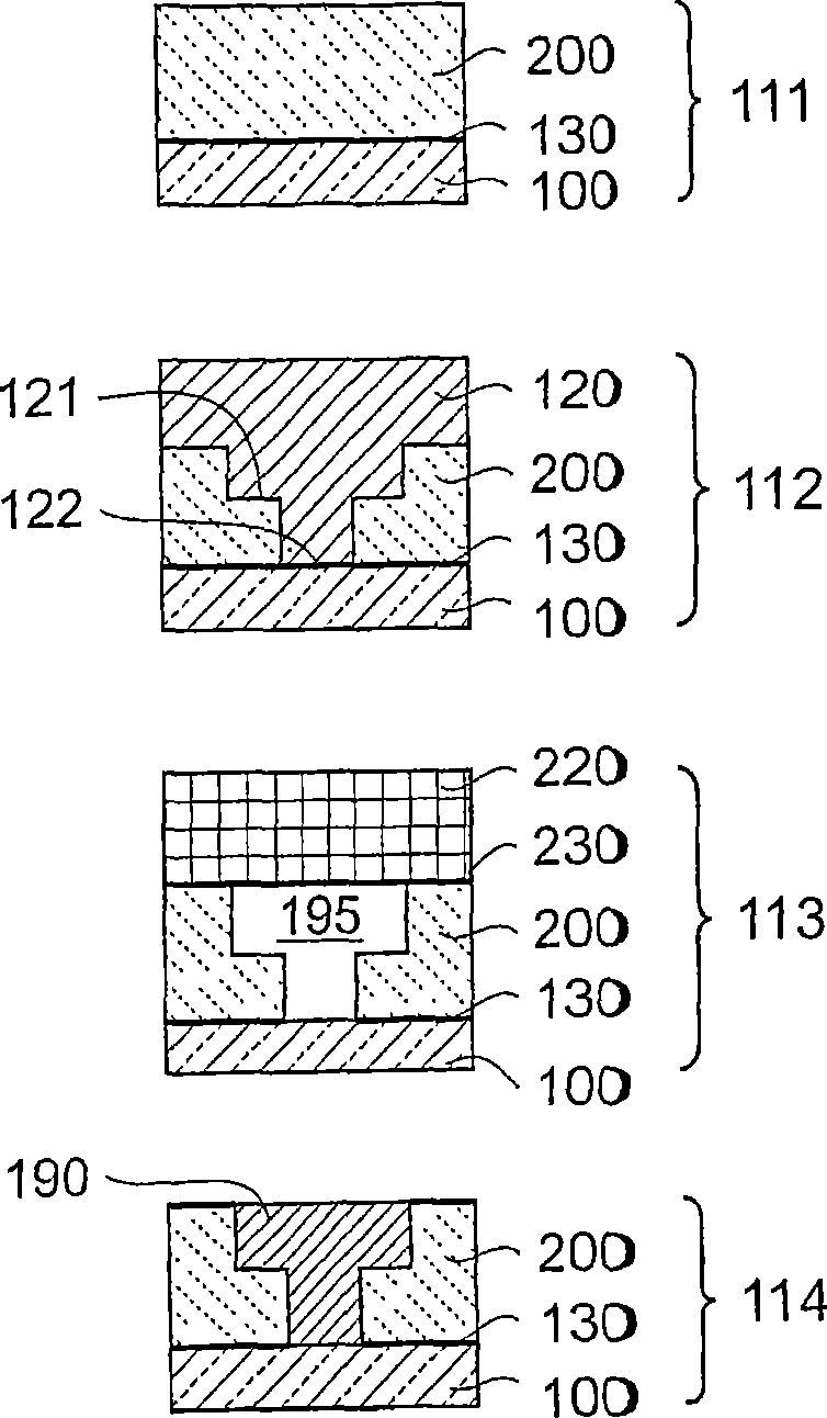
[0019] refer to figure 2 , in one embodiment of the present invention, in step 101 , a diffusion barrier layer 130 is deposited on the substrate 100 . Diffusion barrier layer 130 covers both the dielectric and previously fabricated vias or wiring connections for connection to subsequent attach layers of the device. A first homogeneous dielectric layer 140 is deposited on the diffusion barrier layer 130 . A uniform silicon nitride etch stop layer 150 is deposited on the first dielectric layer 140 . A second uniform dielectric layer 160 is deposited on the etch stop layer 150 . A silicon nitride hard cap layer 170 is deposited on the second dielectric layer 160 . A uniform liquid pre-polymer resist layer 180 is deposited on the hard coat layer 170 . Dielectric layers 140 and 160 may be formed from the SiLK material available from the Dow Chemical Company described above. Deposition of the resist layer 180 can be done by sputter coating, spin coating, pipetting or by a roll...


PUM


Abstract

Described is a method for forming a multilevel structure on a surface. The method comprises: depositing a curable liquid layer (200) on the surface; pressing a stamp (120) having a multilevel pattern therein into the liquid layer to produce in the liquid layer a multilevel structure defined by the pattern; and, curing the liquid layer to produce a solid layer having the multilevel structure therein. Mechanical alignment may be employed to enhance optical alignment of the stamp relative to the substrate via a plurality of spaced protrusions on the substrate on which the structure is to be formed and complementary recesses in the patterning of the stamp.

Description

technical field [0001] The present invention relates generally to fabrication methods for forming multilevel structures, and more particularly to methods for forming conductive structures in substrates. Background technique [0002] In semiconductor manufacturing technology, there is pressure to increase area density and manufacturing speed while reducing manufacturing costs. The shrinkage of semiconductor devices on integrated circuit (IC) chips, especially complementary metal-oxide-semiconductor (CMOS) transistor devices, generally follows Moore's law and is entering the submicron region. The number of devices integrated in an IC chip is on the order of tens of millions and is increasing. The signal interconnection between these devices today consists of many layers of metal interconnections separated from each other by dielectric material. Eight interconnection layers are usually required now. However, the number of layers is expected to increase further. As IC size d...

Claims


Application Information

Patent Timeline
Patent Type & Authority Applications(China)
IPC IPC(8): H01L21/768G03F7/00H01L21/027
CPCB82Y10/00B82Y40/00G03F7/0002H01L21/76807H01L21/76817H01L2221/1021Y10S438/946H01L21/768H01L21/28
Inventor A·比耶池B·麦克尔
Owner INT BUSINESS MASCH CORP
Why Eureka
Try Eureka