Gallium nitride base high brightness high power blue green LED chip

A light-emitting diode, gallium nitride-based technology, applied in electrical components, circuits, semiconductor devices, etc. Large production costs and other issues, to achieve the effect of high power, good reliability, and increased reliability

Active Publication Date: 2006-11-29
DALIAN MEIMING EPITAXIAL WAFER TECH
View PDF0 Cites 8 Cited by
  • Summary
  • Abstract
  • Description
  • Claims
  • Application Information

AI Technical Summary

Problems solved by technology

However, if light-emitting diodes want to obtain high brightness, the current must be well dispersed. The current concentration of existing products due to the smaller size increases the contact resistance, resulting in excessive heat, unstable performance, relatively short life, and insufficient productivity and output. Improve, increase the production cost of the product and other defects
[0004] Chinese patent ZL001313223 ("Manufacturing Method of Gallium Nitride-Based Blue Light-Emitting Diode Chip") has carried out a comprehensive transformation of the manufacturing method, but it cannot completely solve the shortcomings of the above-mentioned products, and cannot truly realize the small-sized, high-brightness, high-power blue light emitting diode chip. Green LED chip

Method used


Image

  • Gallium nitride base high brightness high power blue green LED chip
  • Gallium nitride base high brightness high power blue green LED chip

Examples


Embodiment 1

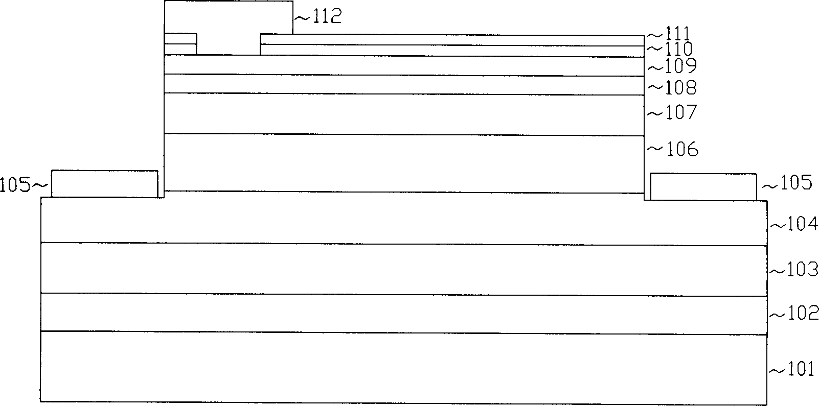
[0034] Refer to attached figure 1 , with figure 2 The structure of the present invention is:

[0035] The longitudinal structure of the gallium nitride series blue-green light LED in the present invention:

[0036] On the upper surface of the sapphire substrate (101), a gallium nitride buffer layer (102) is sequentially grown by MOCVD, on the buffer layer is a gallium nitride substrate replacement layer (103), on the replacement layer is an N-type nitride A gallium layer (104), an active layer (106) above the N-type gallium nitride layer, an aluminum gallium nitride (AlGaN) layer (107) above the active layer, and a P-type nitride layer on the aluminum gallium nitride layer Gallium layer (108), on the P-type gallium nitride layer (108), is heavily doped P + type gallium nitride (109). In heavily doped P + A transparent electrode layer (110) is above the type gallium nitride, and a passivation layer (111) is above the transparent electrode layer; the surface of the passiva...


PUM


Abstract

A blue/ green LED chip of gallium nitride base in high brightness and high voltage type is prepared as utilizing sapphire as substrate and growing multiple layer of GaInN / AIGaN / GaN quantum well structure, covering transparent conductive layer and P and N electrode on stage by utilizing electronic beam evaporation method, applying a photo etching technique to prepare a special horizontal structure of P electrode and N electrode.

Description

technical field [0001] The invention relates to a high-brightness and high-power blue-green light-emitting diode chip, in particular to a gallium nitride-based high-brightness and high-power blue-green light-emitting diode chip with sapphire as a substrate. Background technique [0002] GaN blue-green light-emitting LED is a light-emitting device that converts electrical energy into light energy (spectrum: 510-530nm, 460-470nm) with high efficiency. At present, the manufacturing technology of red, orange and yellow light-emitting LEDs has matured, represented by GaN The third-generation semiconductor materials can emit blue-green light, making up for the color gap; the advantages of blue-green light-emitting diodes represented by GaN in the application field of semiconductor lighting have been highlighted, and have become a research hotspot in this field. [0003] Blue light-emitting diodes have many advantages such as small size, cold light source, f...

Claims


Application Information

Patent Timeline
Patent Type & Authority Applications(China)
IPC IPC(8): H01L33/00H01L33/36H01L33/38
Inventor 王省莲马欣荣陈向东肖志国
Owner DALIAN MEIMING EPITAXIAL WAFER TECH
Why Eureka
Try Eureka