Light-emitting diode structure based on GaN/sapphire transparent substrate and preparation method

A technology of light-emitting diodes and transparent substrates, applied in electrical components, circuits, semiconductor devices, etc., can solve the problems of inability to develop the transparent substrate structure, increase absorption loss, reduce device efficiency, etc., to improve light extraction efficiency and brightness, Reduce absorption, improve pressure drop effect

Inactive Publication Date: 2006-12-27
BEIJING UNIV OF TECH
View PDF0 Cites 14 Cited by
  • Summary
  • Abstract
  • Description
  • Claims
  • Application Information

AI Technical Summary

Problems solved by technology

Due to the existence of gallium arsenide material, it will inevitably reduce the efficiency of the device, reduce the brightness of the device, and cannot take full advantage of the transparent substrate structure
In addition, the mesa structure itself will increase the horizontal series resistance, and a large serie

Method used


Image

  • Light-emitting diode structure based on GaN/sapphire transparent substrate and preparation method
  • Light-emitting diode structure based on GaN/sapphire transparent substrate and preparation method
  • Light-emitting diode structure based on GaN/sapphire transparent substrate and preparation method

Examples


Embodiment Construction

[0057] Specific embodiments of the present invention are described below in conjunction with accompanying drawing:

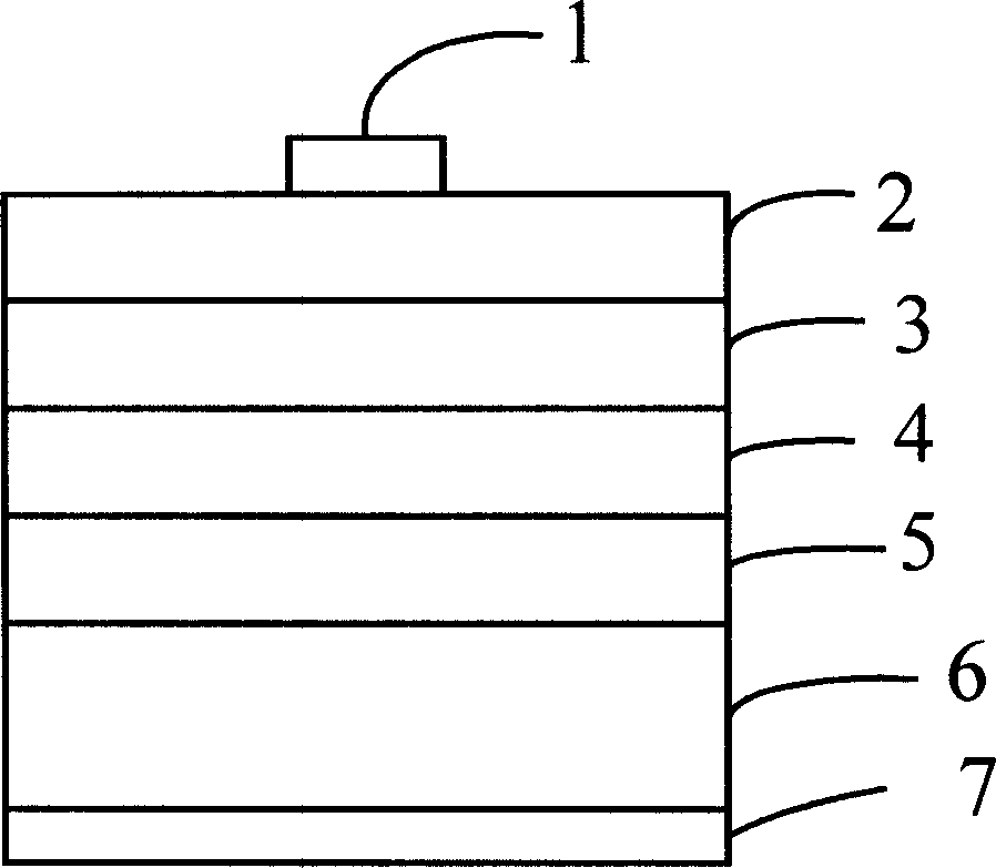
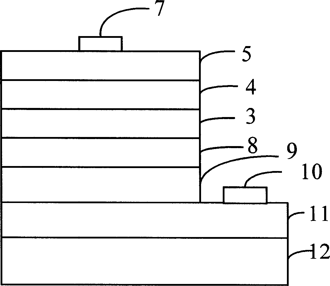
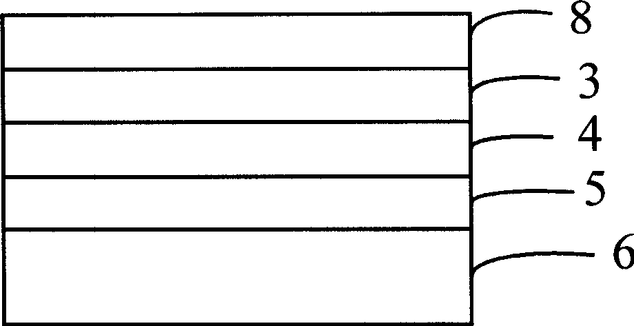
[0058] see figure 2 Shown is the device and structure of the light-emitting diode based on the bonding technology of the present invention and using gallium nitride / sapphire as the transparent substrate, including n-type ohmic contact electrodes 7 and n-type carrier confinement layers stacked vertically in sequence 5. Active region 4, p-type carrier confinement layer 3: under the p-type carrier confinement layer 3, sequentially include a tunnel junction structure 8, a bonding layer 9, a conductive epitaxial layer 11, and a transparent substrate 12; A conductive epitaxial layer ohmic contact electrode 10 is further provided on the upper surface of the conductive epitaxial layer 11 located at the lateral extension portion at the bottom of the bonding layer 9 .

[0059] Wherein, the bonding layer 9 may be a direct bonding of two semiconductor materials, or may re...


PUM


Abstract

The disclosed GaN/sapphire-based transparent-substrate LED comprises vertically: a n-type ohmic contact electrode (7), a n-type carrier limit layer (5), a source area (4), and a p-type carrier limit layer (3), wherein under (3), arranging a tunnel structure (8), a bonding layer (9), a conductive epitaxy layer (11) with an ohmic contact electrode (10), and a transparent substrate (12). The opposite manufacture method comprises: epitaxy growing, bonding, removing substrate, photo etching, eroding, and further processing.

Description

technical field [0001] The invention discloses a structure and a preparation method for preparing a transparent substrate light-emitting diode based on bonding technology, belongs to the field of semiconductor optoelectronic devices, and relates to a structure and preparation technology of a light-emitting diode. Background technique [0002] A light-emitting diode is a semiconductor electroluminescent device that directly converts electrical energy into light energy. Due to its small size, light weight, high efficiency, long life, and environmental protection, it is widely used in large-screen color display, traffic indication, special lighting and other fields. The wavelength range of light-emitting diodes covers the entire visible light band from ultraviolet to infrared, and the materials used involve gallium nitride-based material systems and gallium arsenide-based material systems. At present, AlGaInP / gallium arsenide light-emitting diodes are the main materials used f...

Claims


Application Information

Patent Timeline
IPC IPC(8): H01L33/00H01L33/02
Inventor 郭霞梁庭郭晶顾晓玲林巧明沈光地
Owner BEIJING UNIV OF TECH
Why Eureka
Try Eureka